Key Findings
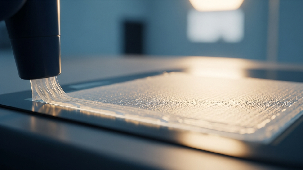
A recent PatSnap Eureka report emphasizes the indispensable role of advanced adhesive technologies and optimized coverage in mitigating cell delamination risks within the semiconductor packaging and display technology sectors. As advanced packaging and flexible displays become thinner and more dense, adhesive performance emerges as a critical determinant of long-term device reliability.
Technical / Clinical Details
The research focuses on improving the flow characteristics of adhesives to ensure uniform application, even over intricate geometries and into micro-gaps, thereby minimizing void formation. This ensures the integrity of the adhesive interface and reduces the risk of delamination. Efforts are also directed at enhancing substrate compatibility to maximize adhesion between dissimilar materials, which is crucial for advanced packaging utilizing diverse materials like polyimide, glass, and metals. Furthermore, developing environmental resistance—including thermal stability and moisture resistance—to maintain adhesive performance under harsh conditions such such as high temperatures, humidity, thermal cycling, and mechanical stress, is a key area of development. Many new adhesive formulations integrate conductive fillers (e.g., silver, carbon nanotubes) or thermal interface materials (TIMs) to provide efficient heat dissipation and improved electrical performance, positioning adhesives as functional materials beyond mere bonding agents.
Background & Context
The semiconductor industry is shifting towards advanced packaging technologies like Fan-Out Wafer-Level Packaging (FOWLP) and 2.5D/3D packaging to achieve higher density and performance, as Moore’s Law approaches its physical limits. Simultaneously, the proliferation of flexible displays and wearable devices drives demand for thin, bendable displays. These technologies necessitate more complex structures and diverse material combinations than conventional packaging, demanding unprecedented reliability and performance from adhesives. Cell delamination directly leads to device malfunction and shortened lifespan, making its prevention a paramount challenge.Strategic Significance & Outlook
Advances in adhesive technology and coverage optimization are essential for the development of next-generation products in advanced packaging and flexible displays. These advancements will enable the creation of smaller, higher-performing, and more reliable electronic devices, accelerating innovations in AI chips, high-speed computing, and foldable smartphones. Moving forward, adhesive manufacturers and device makers are expected to further strengthen collaboration between material science and process technology, focusing on developing more sustainable and high-performance adhesive solutions that resist delamination even under extreme conditions.
Source: https://eureka.patsnap.com/report-optimizing-adhesive-coverage-to-reduce-cell-delamination-risks


Comments