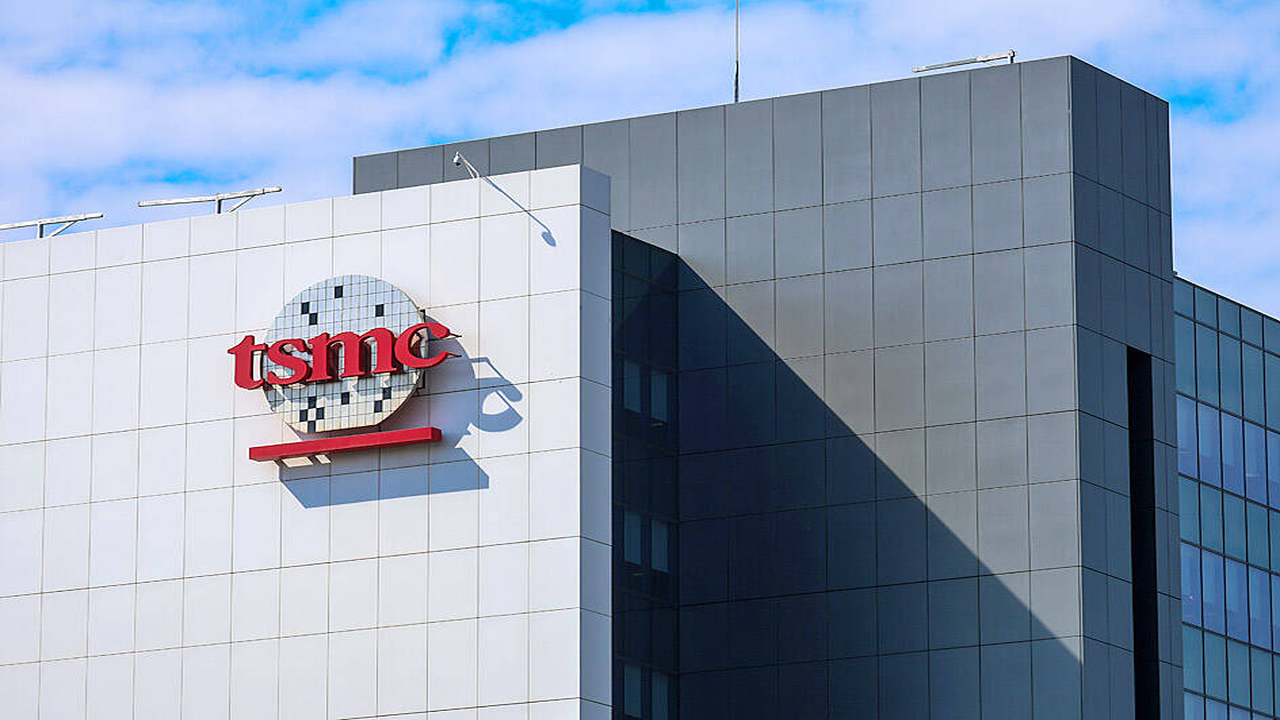
AI Driving Semiconductor Market Growth to $1.5 Trillion
Taiwan Semiconductor Manufacturing Co. (TSMC), the world’s largest contract chipmaker, has issued an optimistic forecast, predicting that the global semiconductor market revenue will hit $1.5 trillion by 2030. This growth is primarily fueled by the explosive demand for artificial intelligence (AI), which is driving unprecedented consumption of tokens and computing power. This projection firmly establishes AI as a central force in next-generation computing and a primary catalyst for semiconductor innovation.
Introducing COUPE: Next-Generation Optoelectronic Integration
In response to AI’s escalating demands for high performance and power efficiency, TSMC is set to introduce its “Compact Universal Photonic Engine (COUPE)” technology later this year. COUPE represents a groundbreaking innovation that integrates multiple integrated circuits (electrical dies), a photonic die, and optical fiber couplers into a single, advanced package. This technology achieves ultra-low impedance and high energy efficiency by directly stacking electrical and photonic dies using SoIC-X stacking. This capability dramatically reduces coupling losses in data centers, boosts energy efficiency, and significantly accelerates chip-to-chip interconnects.
Integration with CoWoS Packaging and Future Outlook
TSMC also plans to integrate its COUPE technology with CoWoS (Chip-on-Wafer-on-Substrate), its leading advanced packaging platform. The third generation of CoWoS is scheduled for volume production this year, with targets to offer even larger CoWoS technologies by 2029—supporting 14 times the reticle size for 24 High Bandwidth Memory (HBM) chips, and over 40 times the reticle size for 64 HBM chips. The integration of COUPE with CoWoS holds immense potential for eliminating chip-to-chip interconnect bottlenecks and substantially improving scalability and performance in future AI/HPC systems. TSMC’s strategy clearly demonstrates that the combination of advanced chiplet technology and optoelectronic integration is indispensable for enhancing AI processor performance and power efficiency, thereby solidifying its leadership in this critical domain.
Source: https://www.taipeitimes.com/News/front/archives/2026/05/15/2003857365


Comments