Background
The rapid advancement of Artificial Intelligence (AI) has created unprecedented demands for computational power and energy efficiency, from data centers to edge devices. However, traditional semiconductor scaling is approaching its physical limits, leading to a slowdown in Moore’s Law. Consequently, to enhance the performance of next-generation AI chips while simultaneously reducing power consumption, the exploration of new materials, innovative process technologies, and fundamentally different device architectures has become indispensable. The United States is accelerating large-scale investments and industry-academia collaborations to maintain its leadership in the semiconductor industry and strengthen its domestic supply chain.
Key Findings / Results
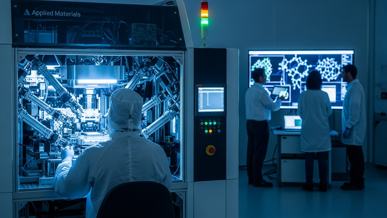
Applied Materials, a global leader in semiconductor manufacturing equipment, has announced that Arizona State University (ASU), Rensselaer Polytechnic Institute (RPI), and Stanford University will join its core R&D hub, the “EPIC (Equipment and Process Innovation and Commercialization) Center” in Silicon Valley, as inaugural research partners.
- Role of the EPIC Center: Located in Silicon Valley, the EPIC Center represents Applied Materials’ largest-ever U.S. investment in advanced semiconductor equipment R&D. Its purpose is to create an ecosystem where university, government, and industry researchers collaborate to accelerate semiconductor technological breakthroughs. A primary mission is to shorten the commercialization timeline from fundamental research to full-scale manufacturing.
- Specifics of Industry-Academia Collaboration: The participating university teams will work closely with Applied Materials’ scientists and engineers to advance research programs in the following areas:
- Advanced Materials: Exploration and development of new functional materials that will dictate the performance of next-generation AI chips.
- Novel Process Technologies: Innovative deposition, patterning, and etching processes that enable further miniaturization and performance enhancement.
- Device Technologies and Chip Architectures: New device structures and chip designs optimized for energy efficiency and computational efficiency.
- Talent Development: This collaboration also provides a robust platform for nurturing highly skilled scientists and engineers who will support the future semiconductor industry. Students will gain practical skills and knowledge through exposure to cutting-edge research environments and industry expertise.
The EPIC Center, backed by a significant $4 billion investment, seeks to halve the time from laboratory breakthrough to full-scale manufacturing, a critical acceleration for the fast-paced semiconductor industry.
Technical Significance & Outlook
This strategic alliance between Applied Materials and leading universities is expected to have a profound impact on the entire semiconductor industry. It will accelerate the development of next-generation AI chips, significantly contributing to improved AI computing performance and reduced energy consumption. Specifically, the following ripple effects are anticipated:
- Evolution of AI Technology: More powerful and energy-efficient AI chips will further accelerate the evolution of various AI applications, including autonomous driving, medical diagnostics, scientific computing, and natural language processing.
- Acceleration of Innovation: Industry-academia collaboration in R&D will quickly translate fundamental research outcomes into industrial applications, shortening the technology innovation cycle. New approaches, such as AI-driven material discovery and process optimization, will be particularly promoted.
- Strengthening of the Domestic Supply Chain: By bolstering the semiconductor R&D ecosystem within the U.S., risks in the global supply chain will be mitigated, and technological self-reliance will be enhanced.
Future challenges include effective collaboration management across multiple organizations, intellectual property sharing and management, and flexible adaptation to rapidly evolving technological trends. Nevertheless, this massive investment and collaboration are undoubtedly essential drivers for achieving the next breakthroughs in semiconductor technology and shaping the future of the AI era.


Comments