Key Findings
Researchers at Cornell University have pioneered a novel method for creating moiré patterns in 2D materials without resorting to the conventional, often challenging, techniques of stacking and twisting. This breakthrough, published in the Proceedings of the National Academy of Sciences, enables the predictable and scalable generation of moiré superlattices by applying controlled strain to layers of molybdenum disulfide (MoS2) via patterned thin films. This innovation fundamentally transforms the approach to engineering quantum materials, making them more accessible for practical applications through standard semiconductor fabrication processes.
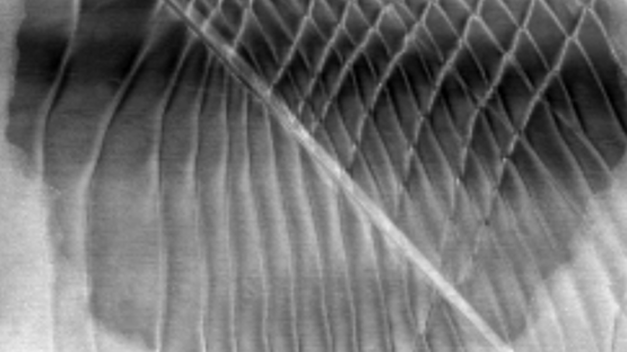
Technical / Clinical Details
- Moiré Superlattices and Quantum Phenomena: Moiré superlattices are emergent periodic structures formed when two crystalline layers with slightly different lattice constants or rotational orientations are overlaid. These superlattices give rise to extraordinary quantum behaviors, including unconventional superconductivity, strongly correlated electron physics, and novel optical properties.
- Limitations of Traditional Methods: Previous methods for creating moiré patterns, such as precisely stacking and twisting 2D material layers (twistronics), are notoriously difficult to control at the nanoscale. Achieving uniform twist angles and high-quality interfaces over macroscopic areas has been a significant hurdle, limiting reproducibility and scalability.
- Strain-Induced Moiré: The Cornell team’s approach involves fabricating patterned thin films on a substrate. When a monolayer of MoS2 is transferred onto this patterned substrate, it conforms to the topography, inducing precise, periodic strain fields within the MoS2. This strain acts as a template to create the desired moiré superlattice without physical stacking or twisting of independent layers.
- Predictability and Scalability: This “strain engineering” method allows for precise control over the moiré pattern’s periodicity, symmetry, and resulting electronic properties, enabling a more deterministic design of quantum materials. Its compatibility with established semiconductor fabrication techniques means it can be scaled up for industrial production, a critical advantage over current methods.
Background & Context
Moiré physics in 2D materials has captivated condensed matter physicists and materials scientists due to its potential to unlock novel quantum states of matter and revolutionize quantum device design. However, the experimental challenges in creating and manipulating these delicate structures have largely confined research to laboratory settings. A scalable and robust fabrication method has been a long-sought goal to bridge the gap between fundamental discovery and technological realization.
Strategic Significance & Outlook
This innovative strain-engineering technique offers a robust and highly scalable pathway for developing quantum materials with tailored properties. Its compatibility with conventional semiconductor fabrication processes has profound implications for the commercialization of quantum technologies. Potential applications include:
- Quantum Computing and Information: Engineering new platforms for qubits and quantum memory with enhanced coherence and control.
- Next-Generation Electronics: Developing ultra-low-power electronic devices, including topological insulators and unconventional superconductors.
- Advanced Sensors: Creating highly sensitive sensors that exploit moiré-induced quantum phenomena for detecting subtle environmental changes.
By simplifying the manufacturing process and improving the predictability of quantum material properties, this research accelerates the transition of moiré 2D materials from a scientific curiosity to a foundational technology, poised to redefine future electronics, energy, and sensing systems.


Comments