Key Findings
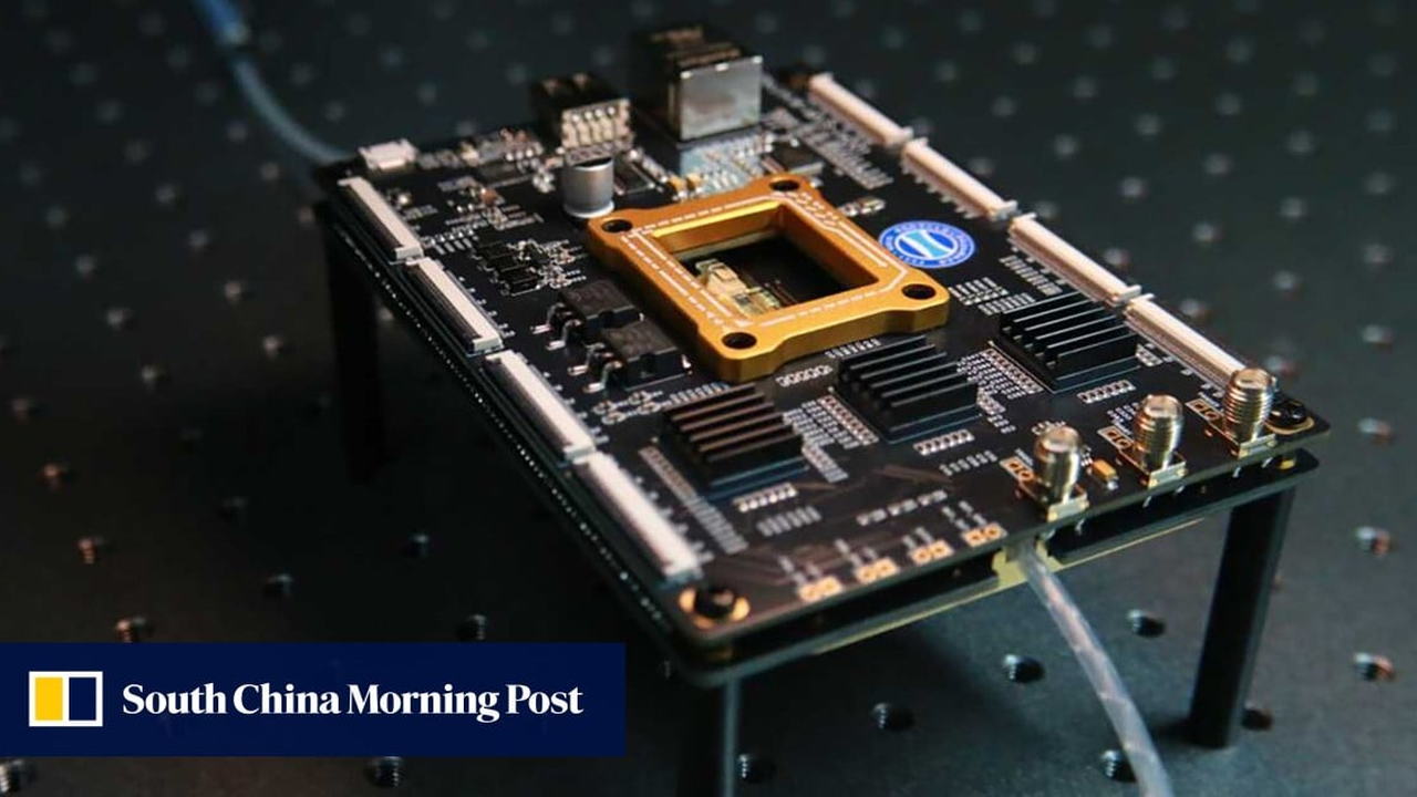
Chinese startup Prinano has announced the successful mass production of photonic chips on 8-inch silicon wafers using its proprietary PL-AS vacuum air-cushion nanoimprint lithography (NIL) equipment, circumventing the need for expensive DUV lithography machines from Dutch firm ASML. This revolutionary technology significantly cuts manufacturing costs by approximately tenfold compared to DUV-based solutions and achieves sub-10nm resolution.
Technical / Clinical Details
Prinano’s PL-AS vacuum air-cushion NIL technology involves directly pressing a master pattern onto a wafer to transfer nanoscale patterns. Unlike conventional photolithography, which relies on a complex multi-step process involving light and photoresist, NIL is based on physical pattern transfer, resulting in a simpler equipment structure and fewer utility requirements. The vacuum air-cushion technique ensures uniform contact between the wafer and the mask, reducing microscopic defects and achieving high yield and reproducibility on large-diameter 8-inch substrates. The company claims the ability to form ultra-fine patterns below 10nm, meeting the resolution requirements for cutting-edge logic semiconductors and photonic devices. Reducing manufacturing costs by a factor of ten is significant, as it lessens reliance on expensive EUV/DUV equipment and drastically improves the economics of semiconductor manufacturing.
Background & Context
Amid escalating global competition in semiconductor manufacturing technology, the United States has tightened export controls on advanced semiconductor equipment to China. ASML’s EUV/DUV lithography machines, in particular, are essential for state-of-the-art semiconductor production, and China faces significant restrictions on their supply. In this context, NIL, as a new lithography technology that does not use light, has been eyed as a strategic alternative for China to build its domestic semiconductor supply chain and reduce external dependence. Prinano’s success marks a major step towards China’s technological self-reliance in this field.
Strategic Significance & Outlook
Prinano’s successful mass production of photonic chips using nanoimprint technology holds profound strategic significance for China’s semiconductor industry, enabling it to counter US export controls and advance technological self-sufficiency. This low-cost, high-resolution manufacturing capability will accelerate the supply of photonic chips, which are seeing growing demand in areas such as data centers, communication networks, and AI accelerators. If this technology can be further scaled up and applied to larger diameter wafers and other types of semiconductor devices, it could significantly impact the global semiconductor market’s competitive landscape. It is expected to particularly provide a strong impetus for the development of China’s domestic semiconductor ecosystem.


Comments