Key Findings
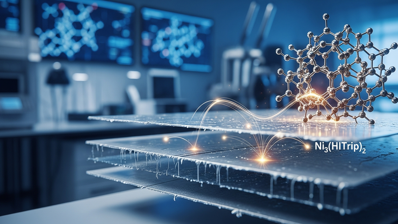
A research team at the Korea Advanced Institute of Science and Technology (KAIST) has made a groundbreaking discovery, developing a novel conductive metal-organic framework (MOF) material, Ni₃(HITrip)₂, which addresses the long-standing challenge of performance degradation in stacked two-dimensional (2D) materials. This new material exhibits unprecedented properties, allowing multi-layered structures to retain the superior electronic characteristics typically observed only in single-layer materials.
Technical / Clinical Details
Conventional stacked 2D materials, such as graphene and MoS₂, suffer from significant device performance degradation due to reduced electron mobility caused by interlayer interactions when multiple layers are assembled. The KAIST team overcame this issue by introducing Ni₃(HITrip)₂. Thanks to its unique molecular structure, Ni₃(HITrip)₂ forms stable conductive pathways between the layers of stacked 2D materials, enabling electrons to move more freely across the layers. This ensures that even in a multi-layered configuration, electrons are not confined within individual layers, and the overall material maintains high electrical conductivity. The research demonstrated that Ni₃(HITrip)₂ dramatically improves electron mobility compared to traditional stacking methods.
Background & Context
2D materials have garnered significant attention for their exceptional electrical, optical, and mechanical properties, making them promising candidates for next-generation electronic devices, sensors, energy storage, and quantum computing. However, the difficulty in fabricating single-layer 2D materials necessitated multi-layering for practical applications. The accompanying performance degradation, however, presented a major bottleneck, hindering their widespread adoption. KAIST’s discovery effectively resolves this bottleneck, making high-density, high-performance 2D material-based electronic devices a realistic possibility. This represents a potential new breakthrough for the semiconductor industry, which is facing limits in conventional microfabrication technologies.
Strategic Significance & Outlook
This new conductive MOF material, Ni₃(HITrip)₂, is expected to find applications in next-generation semiconductor devices, particularly in flexible electronics, transparent electronics, and quantum dot displays and sensors. The approach of precisely controlling interlayer interactions also provides new guidelines for designing functional materials with even more complex multi-layered structures. The KAIST research team aims to further develop this technology and accelerate its industrial translation, maximizing the potential of 2D materials and shaping the future of the electronics industry.
Source: https://www.alphagalileo.org/en-gb/Item-Display?ItemId=273808


Comments