Key Findings: Maximizing AI Chip Performance with New Manufacturing Technologies
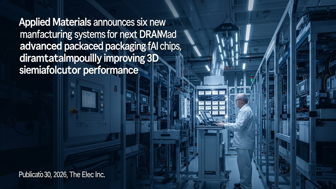
Applied Materials has announced six groundbreaking semiconductor manufacturing systems specifically designed for next-generation DRAM and advanced packaging, critical components for AI processors. These systems aim to dramatically improve the performance and power efficiency of 3D semiconductor devices, directly contributing to enhanced computational power and data transfer speeds in AI chips.
Technical & Clinical Details: Innovations in DRAM and Advanced Packaging
The new portfolio was unveiled at the “2026 DRAM & Advanced Packaging Master Class” on June 25th. Key systems introduced include:
- Epitaxy System for Next-Generation DRAM: This system optimizes the crystal growth process in DRAM manufacturing, leading to increased memory cell density and faster data read/write speeds. This will enable more efficient processing of the vast amounts of data required for AI model training and inference.
- Chemical Mechanical Planarization (CMP) System for Hybrid Bonding Applications: Achieving extremely high wafer surface flatness is paramount for advanced packaging, particularly in 3D stacked structures. The new CMP system employs ultra-precise polishing techniques to significantly improve the accuracy and reliability of hybrid bonding between different wafers, reducing the risk of connection failures in stacked chips.
These technologies were developed to overcome the challenges of miniaturization and 3D integration that have proven difficult with conventional semiconductor manufacturing processes. Through an advanced fusion of materials science and process control, these systems are also expected to contribute to improved yields and reduced manufacturing costs.
Background & Context: Addressing Semiconductor Needs in the AI Era
With the rapid evolution of AI technology, semiconductor chips supporting it demand higher processing power, greater memory capacity, and lower power consumption. Memory technologies such as DRAM and NAND flash are particularly crucial factors determining the performance of AI applications in data centers and edge devices. Leveraging its extensive experience and technological leadership in the semiconductor equipment market, Applied Materials aims to meet these new demands of the AI era with this suite of new systems.
Strategic Significance & Outlook: Strengthening AI Infrastructure and Market Competitiveness
Applied Materials’ announcement signifies a major advancement in the foundational manufacturing technologies for AI chips, amidst an intensifying AI chip development race. The high-performance capabilities of next-generation DRAM and advanced packaging techniques for efficient and reliable chip stacking will directly address bottlenecks in the overall AI infrastructure. This is expected to accelerate the innovation cycle for AI processors, ultimately leading to the market introduction of more powerful and energy-efficient AI products. Semiconductor manufacturers adopting these latest manufacturing systems will further strengthen their competitive edge in the AI chip market.
Source: https://www.thelec.net/news/articleView.html?idxno=11800
Get our weekly technology intelligence — free
Receive an infographic that lets you judge at a glance whether each field’s analysis report is worth reading.
Subscribe Free — Weekly Tech Intelligence
By subscribing, you’ll receive Troy-Technical’s weekly technology intelligence newsletter.
- Your email and selected fields are used only to deliver the newsletter.
- We never share your information with third parties.
- You can unsubscribe anytime via the link in each email.
See our Privacy Policy for details.
Takes about a minute · Unsubscribe anytime