Key Findings
SK Hynix has announced an unprecedented investment plan totaling $64 billion (over 10 trillion JPY) in its domestic memory chip and advanced packaging facilities over the next several years. This monumental investment aims to dramatically boost the production capacity of cutting-edge AI memory chips, such as High Bandwidth Memory (HBM), and the advanced packaging capabilities required to integrate them, thereby strengthening the company’s leadership in the artificial intelligence (AI) memory market.
Technical / Clinical Details
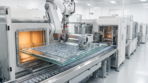
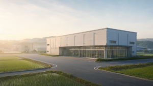
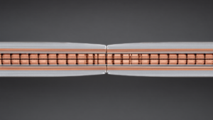
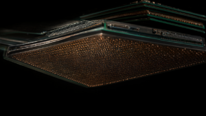
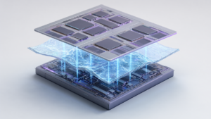
The $64 billion investment will primarily be allocated to two major projects. The first is the construction of a new DRAM production facility, ‘M17.’ M17 will specialize in manufacturing advanced DRAM, including next-generation HBM products, and will incorporate state-of-the-art EUV (Extreme Ultraviolet) lithography technology to maximize production efficiency and yield. The second project involves the expansion of ‘P&T7,’ a dedicated advanced packaging facility. P&T7 will focus on research, development, and mass production of 2.5D/3D packaging technologies like CoWoS (Chip-on-Wafer-on-Substrate), which integrates HBM with AI processors. Specifically, the goal is to enhance HBM’s electrical performance and reliability through the adoption of hybrid bonding technology and improved thermal management solutions.
Background & Context
The increasing complexity of AI models and the explosion of data volumes demand not only immense computational power from AI processors but also extraordinary data bandwidth from connected memory. HBM has emerged as the most effective solution to overcome this bottleneck, with demand skyrocketing from leading AI chip manufacturers such as NVIDIA, AMD, and Intel. As one of the pioneers in the HBM market, SK Hynix has already secured a significant market share with products like HBM3E. This latest investment is a strategic decision to maintain its lead in HBM4 and subsequent generations. The global semiconductor supply chain is facing severe shortages in advanced packaging capacity, and this investment is expected to contribute significantly to stabilizing the supply of AI semiconductors.
Strategic Significance & Outlook
SK Hynix’s colossal $64 billion investment will further solidify its position as a dominant player in the AI-era memory semiconductor market. The construction and expansion of M17 and P&T7 will dramatically increase the company’s production capacity to meet global HBM demand and enable it to maintain its technological edge. This investment is also expected to have ripple effects throughout South Korea’s semiconductor industry, benefiting related equipment and material manufacturers. Long-term, SK Hynix’s HBM technological innovations are anticipated to form the backbone supporting the further evolution of AI and its widespread adoption across various industries.
Source: https://finance.biggo.com/news/e666959f-3828-44a1-b119-5dfdb45f39ad
Get our weekly technology intelligence — free
Receive an infographic that lets you judge at a glance whether each field’s analysis report is worth reading.
Subscribe Free — Weekly Tech Intelligence
By subscribing, you’ll receive Troy-Technical’s weekly technology intelligence newsletter.
- Your email and selected fields are used only to deliver the newsletter.
- We never share your information with third parties.
- You can unsubscribe anytime via the link in each email.
See our Privacy Policy for details.
Takes about a minute · Unsubscribe anytime