Background: The Potential of Metasurfaces and Manufacturing Bottlenecks
Metasurfaces, revolutionary optical devices composed of planar arrangements of sub-wavelength nanostructures, offer unprecedented control over the amplitude, phase, and polarization of light. They hold immense promise for diverse applications such as ultra-thin lenses, holography, stealth technology, and high-sensitivity sensors. However, the high-precision and efficient fabrication of these nanostructures, especially at scale, has been a significant challenge. Electron beam lithography (EBL), the current gold standard for high-resolution patterning, suffers from low throughput and extremely high manufacturing costs, hindering widespread commercialization.
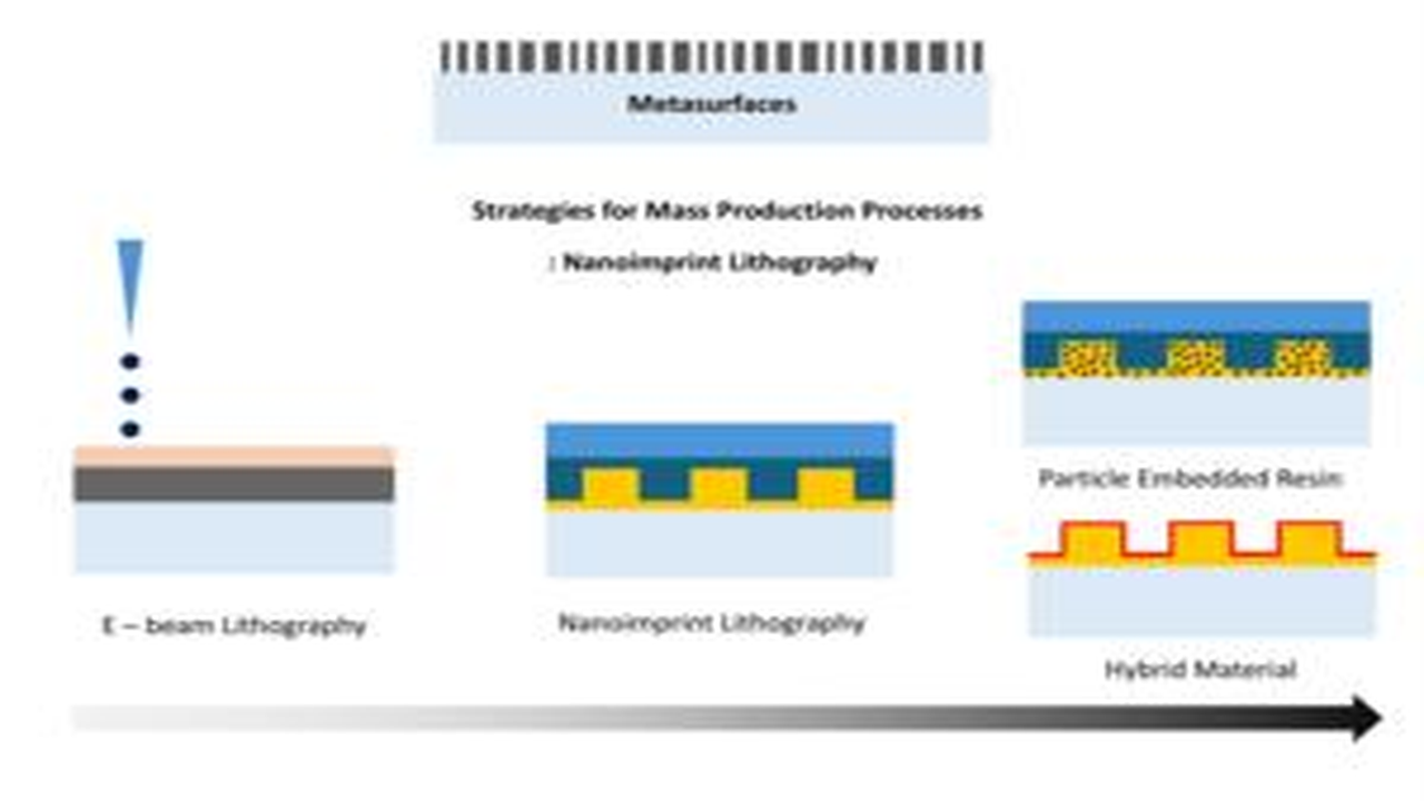
Key Findings / Results: POSTECH’s Innovative Nanoimprint Lithography Strategies
To overcome the limitations of EBL in large-scale metasurface manufacturing, a research team from Pohang University of Science and Technology (POSTECH) has proposed groundbreaking strategies leveraging nanoimprint lithography (NIL). Their findings have been published in Optics and Photonics Research.
The NIL strategies proposed by the POSTECH team primarily address two critical challenges:
- Ensuring Mass Producibility: NIL offers significantly higher throughput and lower cost compared to EBL, as it relies on repetitive pattern transfer from a master mold. This opens a viable pathway for large-scale production, essential for the commercialization of metasurfaces.
- Overcoming the ‘Low Refractive Index’ Problem: Many high-performance metasurfaces rely on high refractive index materials for efficient light manipulation. However, conventional NIL often employs polymer resins with relatively low refractive indices, making it challenging to fabricate high-quality metasurfaces without compromising optical performance.
To address these issues, the research team developed the following innovative approaches:
- Hybrid Material Method: This approach combines the NIL process with atomic layer deposition (ALD). By precisely depositing high refractive index inorganic materials (e.g., TiO2, ZnO) onto NIL-patterned structures, the team can achieve high optical performance while maintaining nanoscale precision. This method leverages the strengths of both patterning and material deposition techniques.
- Particle-Embedded Resins: The researchers also explored the use of NIL resins uniformly dispersed with high refractive index nanoparticles (e.g., barium titanate nanoparticles). This technique directly increases the refractive index of the imprinted structures, mitigating the optical performance deficit without additional deposition steps.
Through these strategies, the POSTECH team has demonstrated a pathway to manufacture metasurfaces with optical performance and efficiency comparable to EBL, but at a significantly more scalable and economically viable level.
Technical Significance & Outlook: Accelerating Commercialization of Next-Generation Optical Devices
The nanoimprint lithography strategies developed by the POSTECH team have the potential to significantly accelerate the commercialization of metasurface technology. By overcoming the primary cost and throughput barriers of EBL, this research makes it feasible to produce lightweight and thin lenses for AR/VR devices, advanced optical modules for next-generation smartphones and automotive sensors, and even highly sensitive biosensors and medical imaging applications.
This technological advancement, driven by manufacturing process innovation, is set to transition groundbreaking optical elements from laboratory curiosities into widespread daily applications. Specifically, NIL’s material flexibility, combined with precision deposition techniques like ALD, is expected to foster the development of diverse, multifunctional metasurfaces, opening new frontiers in optical technology. This positions South Korea as a pivotal player in the manufacturing of next-generation optical devices.


Comments