Key Findings
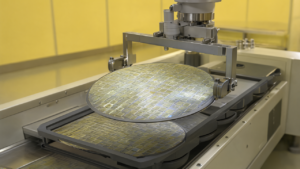
In response to the escalating demand for data transmission bandwidth driven by an explosion in AI computing power, global leading foundries—including TSMC, UMC, GlobalFoundries, and Tower Semiconductor—are significantly accelerating their mass production capabilities and capacity expansion in silicon photonics. Notably, UMC has shipped its first mass-produced silicon photonics wafers from its Singapore fab, and TSMC’s advanced COUPE integrated platform has already entered its production phase.
Technical / Clinical Details
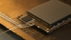
UMC is advancing two silicon photonics strategies, including a 12-inch wafer solution licensed from imec, and has successfully delivered its first volume production wafers from its Singapore facility, aiming to establish a strong foothold in this high-growth market. Concurrently, TSMC’s ‘COUPE’ (Co-Utilized Package) integrated platform combines cutting-edge packaging technologies with silicon photonics to dramatically enhance the efficiency of inter-chip communication critical for AI and high-performance computing (HPC). Furthermore, Tower Semiconductor is proceeding with plans to convert its Arai fab in Japan into a 12-inch silicon photonics and advanced packaging platform, anticipating substantial future capacity expansion. GlobalFoundries is also increasing its 2026 capital expenditure budget and expanding its silicon photonics production capabilities to address the sustained long-term demand from the AI and HPC sectors.
Background & Context
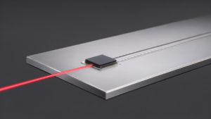
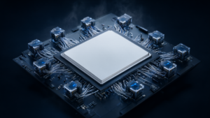
Data centers supporting AI and HPC applications face severe bottlenecks in power consumption and data transmission speeds with conventional copper interconnects, struggling to handle the immense volume of data. Silicon photonics is emerging as a breakthrough technology to overcome these challenges by transmitting optical signals on-chip. The heightened investment from foundries in this domain stems from a shared consensus that AI and HPC will be the long-term growth drivers for the semiconductor industry. Specifically, technologies like Co-Packaged Optics (CPO) are becoming indispensable for next-generation interconnects, making the securing and mass production of foundational silicon photonics technology an urgent priority.
Strategic Significance & Outlook
These large-scale investments and capacity expansions in silicon photonics by major foundries are poised to significantly shape the future of the data center and AI infrastructure markets. With UMC and TSMC entering mass production, and Tower Semiconductor and GlobalFoundries expanding their capacities, the supply of high-performance, energy-efficient optical interconnect solutions is expected to stabilize, and costs are projected to decrease. This will enable the further scaling and complexity of AI models, accelerating developments in applications such as autonomous driving, cloud computing, and quantum computing. Intensified competition among foundries will further stimulate technological innovation, paving the way for silicon photonics to become a new cornerstone of the semiconductor industry.
Get our weekly technology intelligence — free
Receive an infographic that lets you judge at a glance whether each field’s analysis report is worth reading.
Subscribe Free — Weekly Tech Intelligence
By subscribing, you’ll receive Troy-Technical’s weekly technology intelligence newsletter.
- Your email and selected fields are used only to deliver the newsletter.
- We never share your information with third parties.
- You can unsubscribe anytime via the link in each email.
See our Privacy Policy for details.
Takes about a minute · Unsubscribe anytime