Background
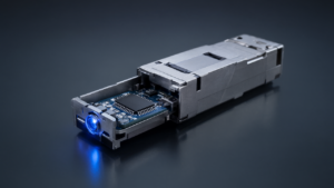
The exponential growth in demand for optical communication and data center capacity necessitates increasingly faster and more energy-efficient optical interconnects and integrated circuits. Silicon photonics (SiP) has become a pivotal platform in this domain, largely owing to its CMOS compatibility, which facilitates cost-effective, large-scale manufacturing. However, silicon intrinsically possesses limitations in efficiently generating and detecting light. This deficiency makes heterogeneous integration with high-performance optical devices, such as III-V semiconductors, a critical and long-standing challenge for SiP. Addressing this, Micro-Transfer Printing (MTP) technology emerges as a scalable and economical solution, representing a significant stride toward realizing the full potential of silicon photonics.
Key Findings
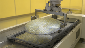
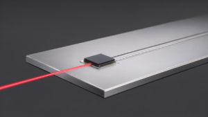
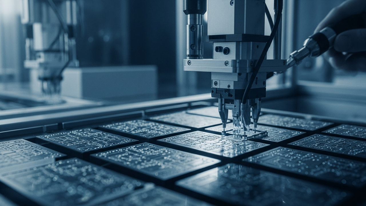
Researchers at Ghent University and imec have conclusively demonstrated Micro-Transfer Printing (MTP) as an exceptionally promising and scalable approach for heterogeneous integration in silicon photonics (SiP). This innovative precision technique allows for the high-accuracy transfer of miniature dies, comprising disparate materials and devices like III-V semiconductor lasers or detectors, onto existing silicon photonic circuits. MTP uniquely combines die-level assembly with efficient wafer-scale processes, thereby enabling the industrial manufacturing of high-performance silicon PICs that leverage both silicon’s excellent manufacturability and the superior optical properties of specialized semiconductor materials. This method offers significant advantages over conventional techniques such as flip-chip bonding or direct growth, including substantially higher throughput and greater flexibility in material selection, crucial for high-density integration and large-scale production demands.
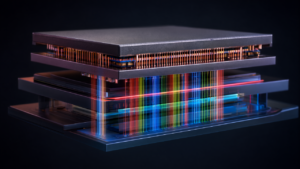
This successful demonstration marks a groundbreaking achievement poised to accelerate innovation across the silicon photonics domain. As MTP technology matures and gains broader industrial adoption, it promises to alleviate critical bandwidth and power efficiency bottlenecks prevalent in AI data centers. Furthermore, it will significantly enhance the performance of next-generation coherent communication systems and enable the development of more complex, high-performance photonic circuits essential for emerging fields like quantum computing and quantum communication. MTP is thus positioned to become a foundational technology, driving higher performance and more cost-effective solutions across diverse photonic application areas and potentially redefining the future landscape of optical technology.
Get our weekly technology intelligence — free
Receive an infographic that lets you judge at a glance whether each field’s analysis report is worth reading.
Subscribe Free — Weekly Tech Intelligence
By subscribing, you’ll receive Troy-Technical’s weekly technology intelligence newsletter.
- Your email and selected fields are used only to deliver the newsletter.
- We never share your information with third parties.
- You can unsubscribe anytime via the link in each email.
See our Privacy Policy for details.
Takes about a minute · Unsubscribe anytime