Key Findings
Intel and Lens Technology have announced a strategic alliance aimed at accelerating innovation in advanced semiconductor packaging technologies, which are essential for the artificial intelligence (AI) era. The primary focus of this collaboration is the development of glass substrate-based packaging solutions, with the goal of achieving exceptionally high performance, enhanced interconnect density, and improved power efficiency required by future AI and data center workloads.
Technical Details
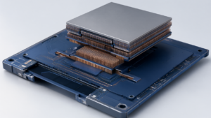
Glass substrates are emerging as a key enabler for next-generation semiconductor packaging due to their superior electrical properties, mechanical stability, and fine-pitch processing capabilities. Compared to traditional organic substrates, glass offers higher wiring density and signal integrity, alongside a lower coefficient of thermal expansion (CTE), which significantly improves reliability in large-scale chiplet integration. Intel and Lens Technology will combine their respective strengths—Intel’s leadership in advanced semiconductor packaging technology and Lens Technology’s expertise in precision manufacturing and glass substrate development—to drive this innovative approach. Specific development objectives include reducing the manufacturing cost of glass substrates, improving yield, and ensuring seamless integration into the existing semiconductor manufacturing ecosystem.
Background & Context
The evolution of AI and data center technologies demands unprecedented levels of performance and efficiency from semiconductor chips. Future processors, potentially housing hundreds of billions of transistors, are encountering physical and electrical limits with conventional packaging technologies. Glass substrate packaging is recognized as a promising solution to overcome these challenges, enabling the integration of more chiplets in close proximity and facilitating ultra-fast data communication. This partnership represents a significant example of U.S. and Chinese companies pooling their specialized expertise to address common technological hurdles in the global semiconductor industry.
Strategic Significance & Outlook
The collaboration between Intel and Lens Technology marks a crucial step in shaping the future of advanced semiconductor packaging. Successful implementation of glass substrate-based solutions is expected to bring breakthroughs in areas such as AI accelerators, HPC processors, and high-performance networking devices. This technology has the potential to alleviate data communication bottlenecks and enable more power-efficient computing platforms, thereby strengthening the foundation of next-generation AI infrastructure. The combined efforts of the two companies are anticipated to establish new standards in semiconductor manufacturing and accelerate the pace of innovation across the industry.
Get our weekly technology intelligence — free
Receive an infographic that lets you judge at a glance whether each field’s analysis report is worth reading.
Subscribe Free — Weekly Tech Intelligence
By subscribing, you’ll receive Troy-Technical’s weekly technology intelligence newsletter.
- Your email and selected fields are used only to deliver the newsletter.
- We never share your information with third parties.
- You can unsubscribe anytime via the link in each email.
See our Privacy Policy for details.
Takes about a minute · Unsubscribe anytime