Key Findings
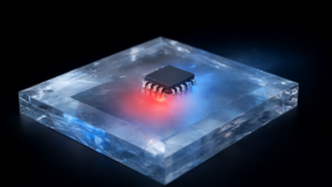
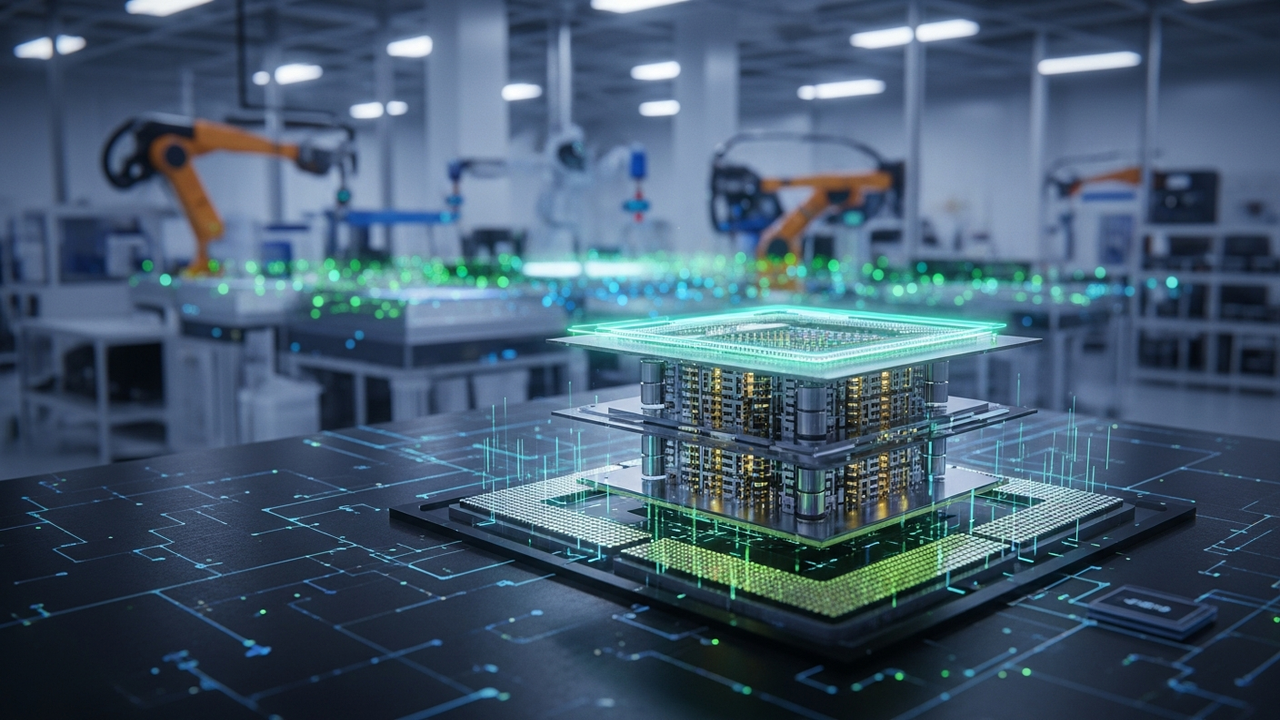
Intel Foundry is powerfully driving the realization of next-generation AI semiconductors through its advanced packaging technologies, developed and deployed at its manufacturing sites within the United States. The company is leveraging innovative techniques such as Foveros stacking, EMIB (Embedded Multi-die Interconnect Bridge) silicon bridges, and EMIB-T to enable chiplet scaling and overcome physical reticle limits, crucial for handling the massive workloads of the AI era.
Technical Details
Intel’s advanced packaging technologies are indispensable for meeting the demands of modern high-performance computing, particularly for AI chips. The key technologies include:
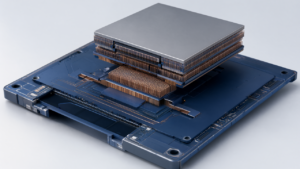
- Foveros Stacking: A technology that vertically stacks multiple chiplets, enabling ultra-high-density 3D integration. This allows for the compact integration of chips with different functions—such as processors, memory, and I/O—significantly improving power efficiency and performance. Foveros Direct further enhances connection density and reduces resistance.
- EMIB Silicon Bridges: A technology that places multiple chiplets adjacent to each other on a planar surface, providing ultra-short-distance, high-bandwidth interconnections. This minimizes communication latency between chiplets and enables extensive chiplet integration. EMIB-T is an evolved form of EMIB designed for even higher I/O density.
- Chiplet Scaling: Processing large-scale AI models requires immense computational units and memory, which are technically and economically challenging to achieve with a single monolithic chip. Chiplet technology solves this by modularly combining smaller chips with different functionalities, allowing for flexible design and cost-effective manufacturing.
- Overcoming Reticle Limits: To build processors with greater computational power beyond the physical limits of lithography equipment (reticle size) in semiconductor manufacturing, multi-die packaging using chiplets is essential.
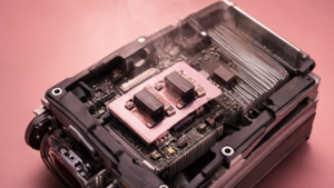
These technologies play a critical role in today’s multi-chip packaging for technology products, seamlessly interconnecting multiple specialized chips to function as if they were a single, powerful unit.
Background & Context
The rapid advancement of AI has placed unprecedented demands on the semiconductor industry for performance and efficiency. As the pace of traditional silicon scaling (Moore’s Law) slows, advanced packaging has emerged as a key enabler for enhancing the performance of next-generation AI accelerators, data center CPUs, and GPUs. Intel’s significant investment in these advanced technologies within the United States aligns with national goals of strengthening the resilience of the U.S. semiconductor supply chain and promoting technological self-sufficiency.Strategic Significance & Outlook
The progress in Intel Foundry’s advanced packaging technologies in the U.S. will further accelerate innovation in the AI sector. The realization of higher-performance and more power-efficient AI semiconductors will drive the development of a wide range of AI applications, including autonomous driving, natural language processing, image recognition, and scientific computing. Through these technologies, Intel aims to boost the competitiveness of its foundry business and play a central role in the global semiconductor manufacturing ecosystem. In the future, these packaging technologies are expected to enable more complex and larger-scale AI systems, forming the foundation for new technological breakthroughs and maintaining a competitive edge in the global market.
Get our weekly technology intelligence — free
Receive an infographic that lets you judge at a glance whether each field’s analysis report is worth reading.
Subscribe Free — Weekly Tech Intelligence
By subscribing, you’ll receive Troy-Technical’s weekly technology intelligence newsletter.
- Your email and selected fields are used only to deliver the newsletter.
- We never share your information with third parties.
- You can unsubscribe anytime via the link in each email.
See our Privacy Policy for details.
Takes about a minute · Unsubscribe anytime