Key Findings
A*STAR Research Entities in Singapore are accelerating the development of package-level optical interconnects, which are essential for realizing advanced Co-Packaged Optics (CPO) platforms. As part of this strategic initiative, the institution has opened a recruitment drive for a Senior Scientist to lead research and development in this cutting-edge technology.
Technical / Clinical Details
The Senior Scientist role encompasses a wide range of responsibilities, focusing on the design, simulation, and wafer-scale integration of optical interconnect technologies. Specifically, the following technical areas are included in the primary duties:
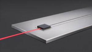
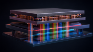
- **Optical Coupling Schemes and Lens Design**: Developing efficient optical coupling schemes for various advanced packaging methods, such as fan-out silicon interposers, polymer glass, or 3D stacking techniques, and designing corresponding lenses. This aims to minimize optical signal loss between chips.
- **Accurate Estimation of Optical Losses**: Performing precise estimations of insertion loss and coupling loss across the entire optical interconnect path to optimize performance.
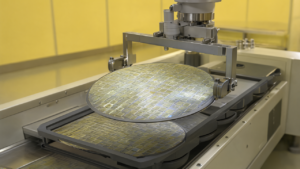
- **Wafer-Scale Integration for Multi-Chiplet Systems**: Contributing to the process development for achieving high-precision optical interconnects at the wafer level in CPO systems integrating multiple chiplets.
- **Simulation and Modeling**: Conducting simulations of optical behavior, thermal characteristics, and mechanical stress to optimize designs and resolve issues.
This position requires deep knowledge of leading photonic packaging platforms, including Silicon Photonics (SiPh), Indium Phosphide (InP), and Thin-Film Lithium Niobate (TFLN), along with expertise in wafer-level process technologies and passive alignment techniques. This indicates A*STAR’s pursuit of comprehensive CPO solutions that integrate diverse materials and technologies.
Background & Context
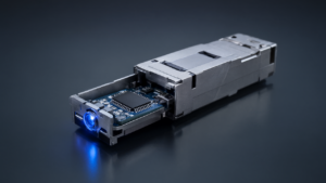
Driven by the increasing demand for AI and High-Performance Computing (HPC), the data transfer bandwidth between processors in data centers is growing exponentially, making it challenging for traditional electrical interconnects to meet these requirements. Co-Packaged Optics (CPO) is gaining attention as an innovative technology that integrates electronic chips and optical transceivers within the same package, significantly shortening data transfer distances and reducing power consumption and latency. Singapore, with its advanced semiconductor manufacturing and R&D capabilities, aims to play a crucial role in the development of next-generation technologies like CPO. This initiative by A*STAR is seen as part of a national strategy to strengthen Singapore’s position as a hub for photonics and packaging technology in the Asia-Pacific region.
Strategic Significance & Outlook
This aggressive CPO development by A*STAR Research Entities demonstrates Singapore’s clear ambition to be at the forefront of global optical integration technology. The recruitment of Senior Scientists will accelerate the resolution of CPO technology bottlenecks (particularly high-efficiency optical coupling and wafer-scale mass production techniques), contributing to the realization of high-performance and energy-efficient optical interconnect solutions in AI data centers. In the future, these research outcomes are expected to disseminate not only within Singapore but also globally across the semiconductor and optical communication industries, fostering the standardization and widespread adoption of CPO technology.
Get our weekly technology intelligence — free
Receive an infographic that lets you judge at a glance whether each field’s analysis report is worth reading.
Subscribe Free — Weekly Tech Intelligence
By subscribing, you’ll receive Troy-Technical’s weekly technology intelligence newsletter.
- Your email and selected fields are used only to deliver the newsletter.
- We never share your information with third parties.
- You can unsubscribe anytime via the link in each email.
See our Privacy Policy for details.
Takes about a minute · Unsubscribe anytime