Key Findings
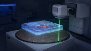
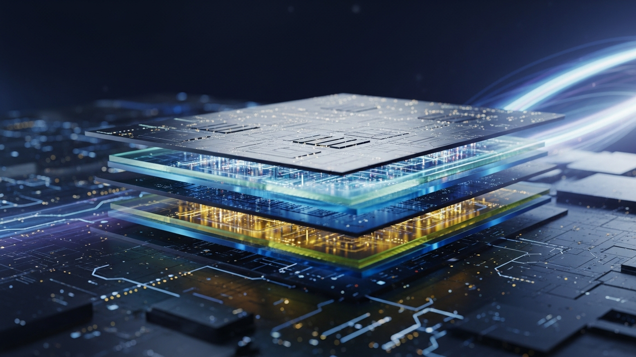
Samsung unveiled an ambitious vision for future AI infrastructure at the Flash Memory Summit (FMS) 2026, introducing a next-generation HBM roadmap encompassing HBM4E and HBM5, and a groundbreaking AI memory architecture dubbed ‘zHBM.’ This zHBM concept aims to revolutionize AI processing by integrating logic and memory in a true 3D fashion, significantly reducing the physical distance for data movement. The solution is specifically designed to alleviate the persistent data transfer bottlenecks observed in conventional systems, promising a dramatic leap in AI computational efficiency.
Technical / Clinical Details
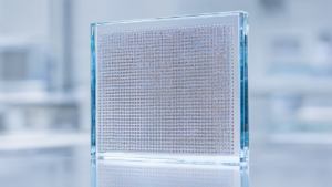
The zHBM architecture moves beyond traditional HBM stacks, which primarily consist of vertically stacked DRAM dies connected to a logic die. Instead, zHBM envisions direct 3D integration of specific logic functionalities either within the HBM stack itself or in its immediate vicinity. This tight integration minimizes the physical distance and latency of data transfer between DRAM and the main processor, a critical factor for AI workloads. While current HBM technologies connect through silicon interposers, zHBM’s closer integration promises to drastically increase effective data bandwidth and improve power efficiency. The forthcoming HBM4E and HBM5 iterations will further enhance bandwidth through increased data channel counts and faster interface speeds, meeting the escalating performance demands of AI accelerators. These advancements are poised to fundamentally address the compute-memory data transfer bottleneck, especially critical for training large language models (LLMs) and complex neural networks.
Background & Context
As AI workloads, particularly deep learning models, continue to scale in computational complexity, the speed of data transfer between processors and memory (memory bandwidth) has become a primary limiting factor for overall system performance. HBM technology was developed precisely to alleviate this bottleneck and has seen widespread adoption in AI GPUs and High-Performance Computing (HPC) applications. However, even with the advent of HBM3E, the relentless pace of AI innovation demands even greater bandwidth and efficiency. Samsung’s initiatives with zHBM and next-generation HBM are a direct response to these market requirements, forming a strategic pillar to bolster its competitiveness in the AI semiconductor market. Rival companies are also actively pursuing advanced memory and 3D integration solutions, making this a crucial battleground in the semiconductor industry.
Strategic Significance & Outlook
3D integrated memory architectures like zHBM are set to become indispensable components in future AI system designs. Resolving data movement bottlenecks directly translates to shorter AI model training times, improved inference efficiency, and the feasibility of building larger, more complex AI models. Samsung aims to solidify its leadership in the AI era by offering comprehensive turnkey solutions that integrate its foundry, memory, and advanced packaging expertise. The industry will closely watch how zHBM is implemented in AI accelerators and its real-world performance validation. This technology holds the potential to revolutionize not only AI but also a broad spectrum of applications including HPC and edge AI devices.
Get our weekly technology intelligence — free
Receive an infographic that lets you judge at a glance whether each field’s analysis report is worth reading.
Subscribe Free — Weekly Tech Intelligence
By subscribing, you’ll receive Troy-Technical’s weekly technology intelligence newsletter.
- Your email and selected fields are used only to deliver the newsletter.
- We never share your information with third parties.
- You can unsubscribe anytime via the link in each email.
See our Privacy Policy for details.
Takes about a minute · Unsubscribe anytime