Key Findings
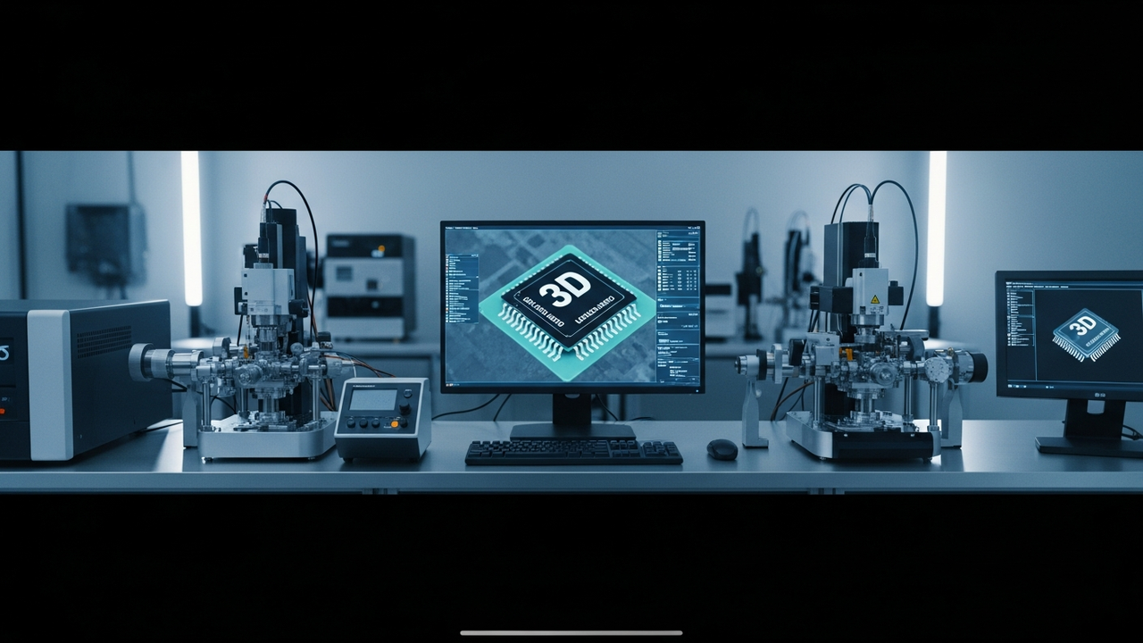
Park Systems has committed substantial investment to its advanced nanoscale metrology portfolio to support 3D packaging and logic research, which are critical for next-generation electronics. This strategic move aims to address the challenges of miniaturization in semiconductor manufacturing, thereby strongly propelling industry-wide technological innovation.
Technical / Clinical Details
Central to this investment is the further enhancement of Atomic Force Microscopy (AFM) technology and the development of integrated nanoscale metrology solutions. Park Systems’ AFMs offer unparalleled capabilities for non-destructive evaluation of surface topography, roughness, and material properties at sub-nanometer resolutions. This performance is crucial for complex 3D logic devices such as 3D stacked structures and gate-all-around (GAA) transistors. The enhanced portfolio will enable high-precision detection and analysis of physical defects, material heterogeneities, and interlayer alignments within these advanced structures. This capability will accelerate problem identification during R&D phases, optimize manufacturing processes, and ultimately improve the reliability and performance of final products.
Background & Context
3D packaging is a vital technology for achieving performance improvements and miniaturization in the semiconductor industry, which faces the physical limits of Moore’s Law. Miniaturization of logic devices now demands not only planar advancements but also vertical stacking and innovative transistor architectures. These advanced structures pose significant challenges for traditional metrology techniques, making high-precision nanoscale 3D measurement indispensable. Park Systems has long been a pioneer in AFM technology, providing solutions across semiconductors, materials science, and biology.
Strategic Significance & Outlook
This strategic investment by Park Systems is expected to play a crucial role in accelerating the development of next-generation semiconductor devices and paving the way for their mass production. Enhanced metrology capabilities directly translate to improved product reliability and reduced development costs, robustly supporting technological innovation in cutting-edge fields like AI, IoT, and high-performance computing. The company plans to continue expanding the frontiers of nanoscale metrology through ongoing R&D, contributing to the advancement of the global electronics industry.
Source: #


Comments