Key Findings
TSMC is dramatically scaling up its advanced packaging capabilities, specifically for CoWoS (Chip-on-Wafer-on-Substrate) and SoIC (System-on-Integrated-Chips) technologies, to address the insatiable demand for AI accelerators. The company plans to boost CoWoS production capacity to more than 120,000-130,000 wafers per month by the end of 2026, a more than tenfold increase from late 2023 levels. However, this aggressive expansion is still anticipated to be outstripped by the explosive growth in AI chip demand. Concurrently, TSMC is accelerating the development of CoPoS, a panel-level packaging technology utilizing glass substrates, aiming for mass production between 2028 and 2029.
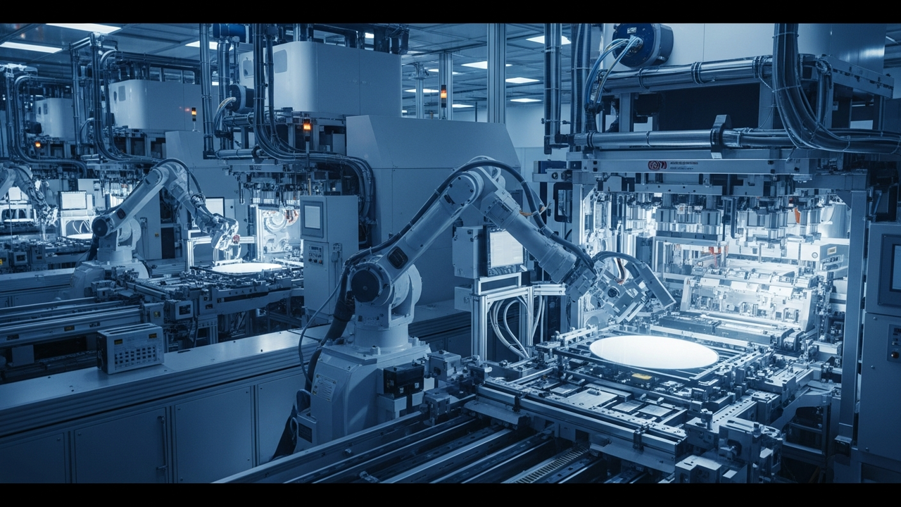
Technical Details
TSMC’s strategy centers on its 2.5D and 3D packaging solutions. CoWoS integrates logic chips and High Bandwidth Memory (HBM) onto a silicon interposer, significantly enhancing data transfer speeds and power efficiency, critical for modern AI workloads. Variations such as CoWoS-S, CoWoS-R, and CoWoS-L are tailored for leading customers like AMD, NVIDIA, and Apple. SoIC, a more advanced 3D stacking technique, enables direct die-to-die bonding at the wafer level, creating ultra-high-density interconnects. The AP7 site in Chiayi is being developed as TSMC’s largest advanced packaging campus, primarily leveraging SoIC for NVIDIA’s next-generation GPUs, while AP8 is expected to exceed 40,000 CoWoS wafers per month by late 2026.
Furthermore, TSMC’s investment in glass-core substrates for its CoPoS technology represents a significant leap forward. Glass substrates offer superior dimensional stability, lower coefficient of thermal expansion (CTE), and finer interconnect capabilities compared to traditional organic substrates. This allows for higher-density chip integration, improved thermal management, and enhanced signal integrity, ultimately boosting AI chip performance and potentially reducing manufacturing costs. This transition is crucial for overcoming the physical limitations of current organic interposers and meeting future performance requirements.
Background and Context
The proliferation of AI applications has made advanced packaging a critical bottleneck in the semiconductor supply chain, with memory and packaging now accounting for 60-70% of AI chip costs. NVIDIA, a dominant player in the AI accelerator market, reportedly secures approximately 60% of TSMC’s CoWoS capacity, creating supply constraints for other companies and slowing the overall deployment of AI infrastructure. This ongoing shortage underscores the strategic importance of packaging capacity. TSMC’s roadmap involves tight collaboration with HBM suppliers, substrate vendors, OSAT partners, and toolmakers to ensure a robust and integrated ecosystem capable of sustaining AI’s rapid growth.
Strategic Significance and Outlook
The aggressive capacity expansion by TSMC, combined with its innovation in technologies like CoPoS, is pivotal for unlocking future advancements in AI and high-performance computing. While immediate supply relief remains challenging due to persistently high demand, these investments are foundational for the long-term growth of the AI industry. The shift towards glass-core substrates and panel-level packaging promises to deliver significant improvements in power efficiency, bandwidth, and cost-effectiveness, paving the way for even more powerful and complex AI systems. TSMC’s leadership in this domain will continue to dictate the pace of innovation across the broader semiconductor landscape, influencing everything from data centers to edge AI applications.


Comments