Key Findings
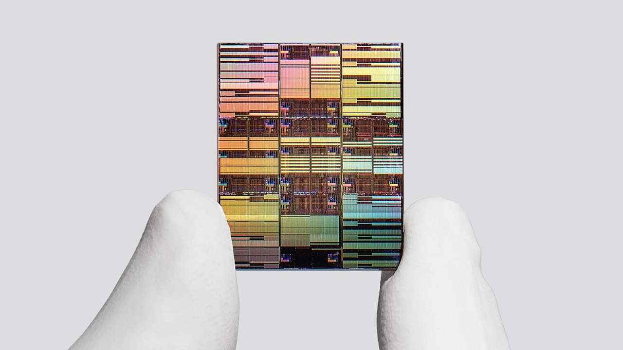
IBM has unveiled “NanoStack,” a revolutionary semiconductor technology that extends chip scaling into the sub-1 nanometer realm to meet the escalating demands of AI workloads. This groundbreaking 3D architecture, which involves vertically stacking transistors, achieves astonishing results: up to a 50% performance improvement or a 70% reduction in energy consumption compared to current 2 nm process technology. NanoStack represents a pivotal breakthrough for significantly boosting the computational power and efficiency of AI chips, addressing critical bottlenecks in AI processing within data centers and cloud environments.
Technical / Clinical Details
NanoStack technology breaks through the limitations of conventional planar transistor layouts, bringing a new dimension to chip design. Its key technical features include:
- Sub-1 nm Node Scaling: It achieves miniaturization below 1 nm, a feat previously considered challenging on conventional roadmaps. This is made possible by innovative advancements in precise material control and manufacturing process technology at the atomic level.
- 3D Transistor Stacking: NanoStack dramatically increases transistor density per chip area by stacking transistors not only horizontally but also vertically. This shortens signal propagation distances, simultaneously achieving higher speeds and lower power consumption. This marks a significant leap from the primarily planar layouts of current 2 nm technology.
- Performance Enhancement and Energy Efficiency: According to IBM’s announcement, this technology offers one of the following benefits:
- Up to 50% Performance Improvement: Delivers up to a 50% increase in processing speed compared to the 2 nm process at the same power consumption level. This significantly reduces the time required for AI model training and inference, enabling the execution of more complex AI tasks.
- Up to 70% Power Consumption Reduction: Achieves up to a 70% reduction in energy consumption while maintaining equivalent performance. Data centers consume immense amounts of power, so this reduction significantly contributes to lower operating costs and reduced environmental impact.
- Fusion of Materials Science and Manufacturing Processes: The realization of NanoStack requires the integration of multiple materials science and process technologies, including new channel materials (e.g., 2D materials, nanosheets), high-k gate dielectrics, and precise etching and deposition techniques. IBM has conducted extensive R&D in these areas for years.
This technology not only enhances AI chip performance but also holds the potential to further improve overall system efficiency through integration with high-bandwidth memory (HBM) and chiplet technologies.
Background & Context
With the rapid proliferation of generative AI and large language models (LLMs), AI workloads are exploding. These AI applications demand enormous computational power and memory bandwidth, making continuous improvement in semiconductor chip performance essential. However, silicon-based semiconductor technology is approaching the physical limits of Moore’s Law, and performance gains from traditional scaling alone are plateauing. IBM’s 3D stacking technologies like NanoStack are anticipated as ‘post-Moore’ solutions that overcome these physical limits and bring new growth trajectories to the semiconductor industry. This is a critical factor for establishing technological advantage in an increasingly competitive global AI landscape.
Strategic Significance & Outlook
IBM’s NanoStack technology holds the potential to redefine the future of AI chip design. Moving forward, this technology is expected to be applied not only to AI chips but also to a wide range of fields, including high-performance computing (HPC), cloud infrastructure, and edge AI devices. The introduction of NanoStack is also expected to accelerate technological innovation across the entire semiconductor manufacturing supply chain. Materials scientists will focus on exploring and integrating more optimal materials, while process engineers will concentrate on establishing more precise manufacturing techniques. This breakthrough is anticipated to accelerate a future where AI can perform more complex tasks faster and more environmentally friendly, contributing to solving various societal challenges such as autonomous driving, personalized medicine, and climate change modeling.
Get our weekly technology intelligence — free
Receive an infographic that lets you judge at a glance whether each field’s analysis report is worth reading.
Subscribe Free — Weekly Tech Intelligence
By subscribing, you’ll receive Troy-Technical’s weekly technology intelligence newsletter.
- Your email and selected fields are used only to deliver the newsletter.
- We never share your information with third parties.
- You can unsubscribe anytime via the link in each email.
See our Privacy Policy for details.
Takes about a minute · Unsubscribe anytime


Comments