
Key Findings
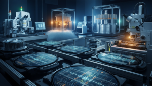
Nokia has announced a substantial expansion of its semiconductor Advanced Test and Packaging (ATP) operations in Allentown, Pennsylvania. This major investment is designed to bolster domestic production capacity for optical networking technologies, critical for scalable AI infrastructure. Nokia plans to increase the site’s production capacity by up to 10 times and nearly double its workforce in Pennsylvania.
Technical and Market Details
This expansion is specifically aimed at addressing the increasing demand for high-performance optical modules and photonic integrated circuits (PICs) for AI data centers and 5G infrastructure. The ATP facility will play an essential role in the testing and packaging of advanced optical technologies such as Co-Packaged Optics (CPO) and Near-Package Optics (NPO). These technologies involve highly complex integration of electrical and optical signals, demanding ultra-precise alignment and reliable packaging.
Nokia’s investment in semiconductor test and packaging aims to strengthen domestic production capabilities within the optical component supply chain, enhancing resilience against geopolitical risks and supply chain disruptions. This will allow Nokia to improve the competitiveness of its optical networking products and provide more reliable, high-performance optical connectivity solutions to AI-related enterprises. Specifically, the facility will test and package Nokia’s cutting-edge coherent optical engines (e.g., ICE7), supporting the demand for 800G and 1.6T modules in AI data centers.
Background and Industry Context
The explosive growth of generative AI is dramatically increasing data center traffic and power consumption, driving an unprecedented demand for optical communication technologies. AI workloads require vast amounts of data to be moved at high speeds with low latency between GPU clusters, making optical interconnects indispensable for resolving computing power bottlenecks in the AI era. Initiatives like the U.S. CHIPS Act are promoting the domestic manufacturing of semiconductors, and Nokia’s investment can be seen as part of this broader strategy.
Strategic Significance and Outlook
Nokia’s expansion of its semiconductor ATP operations in Pennsylvania clearly indicates the growing importance of domestic production in building AI infrastructure. The up to 10x increase in production capacity and doubling of employment underscore Nokia’s commitment to the rapid growth of the AI market. This investment will accelerate innovation in optical networking technologies and play a crucial role in improving the performance and energy efficiency of AI data centers. In the future, this initiative is expected to strengthen the U.S. semiconductor ecosystem and solidify the foundation of digital infrastructure in the AI era.
Get our weekly technology intelligence — free
Receive an infographic that lets you judge at a glance whether each field’s analysis report is worth reading.
Subscribe Free — Weekly Tech Intelligence
By subscribing, you’ll receive Troy-Technical’s weekly technology intelligence newsletter.
- Your email and selected fields are used only to deliver the newsletter.
- We never share your information with third parties.
- You can unsubscribe anytime via the link in each email.
See our Privacy Policy for details.
Takes about a minute · Unsubscribe anytime


Comments