Key Findings
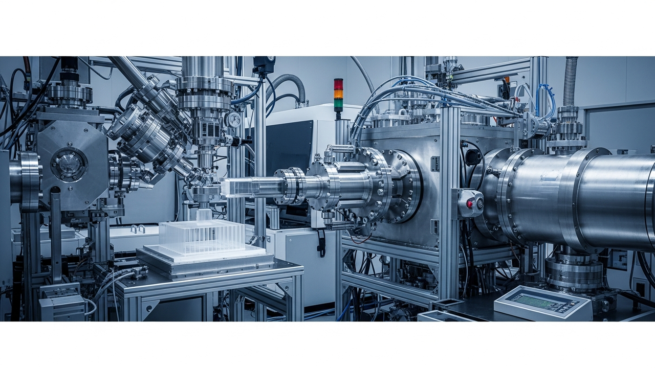
Chemical Vapor Deposition (CVD) stands as a critically important thin-film deposition technique for manufacturing high-quality and high-performance solid materials. This process is extensively utilized in the semiconductor industry, enabling the precise formation of conductive, insulating, or semiconducting thin films ranging from tens to hundreds of nanometers up to several micrometers. CVD technology forms the foundational pillar supporting the performance and reliability of modern electronic devices, with Plasma-Enhanced CVD (PECVD) significantly enhancing the flexibility of semiconductor manufacturing processes by enabling deposition at lower temperatures.
Technical Details
The CVD process is based on the principle of introducing volatile precursor gases into a reaction chamber, where they undergo chemical reactions on a substrate surface to deposit a solid thin film. These reactions can be driven by various energy sources, including heat (thermal CVD), plasma (PECVD), or light (photo-CVD). PECVD, by activating precursor gases through plasma, allows for film deposition at relatively lower temperatures, minimizing damage to heat-sensitive substrates or existing device structures. This greatly expands the applicability of CVD in manufacturing complex semiconductor devices with multi-layered structures. The deposited thin films exhibit excellent density, uniformity, and compositional control, making CVD useful for depositing various materials such as silicon nitride (SiN), silicon dioxide (SiO2), polysilicon, tungsten, and aluminum.
Background & Context
The semiconductor industry continually advances device miniaturization and integration in line with Moore’s Law, demanding extremely precise material processing technologies. CVD is one of the central techniques for forming various functional layers in sub-micron to nano-scale semiconductor devices, including gate dielectrics, interconnect layers, and passivation films for transistors. Particularly in advanced devices like 3D NAND flash memory and high-performance logic ICs, uniform film deposition onto complex topographical structures is required, and CVD’s advanced control capabilities make this possible. The continuous evolution of CVD technology also contributes to reducing semiconductor manufacturing costs and improving yields.
Strategic Significance & Outlook
Chemical Vapor Deposition (CVD) technology will continue to be a crucial driving force for innovation in the semiconductor industry. Its role is expected to increase further with ongoing miniaturization, the introduction of new materials (e.g., 2D materials and high-k dielectrics), and the formation of more complex 3D structures. Combinations with related technologies like Atomic Layer Deposition (ALD), alongside the introduction of new plasma sources and in-situ monitoring techniques, will further enhance CVD process control and efficiency. This will provide the essential material foundation for realizing ultra-high-performance semiconductor devices that underpin next-generation technologies such as AI, 5G, autonomous driving, and quantum computing. CVD remains a dynamic research field that continues to push the boundaries of materials science and engineering.
Source: https://en.wikipedia.org/wiki/Chemical_vapor_deposition
Get our weekly technology intelligence — free
Receive an infographic that lets you judge at a glance whether each field’s analysis report is worth reading.
Subscribe Free — Weekly Tech Intelligence
By subscribing, you’ll receive Troy-Technical’s weekly technology intelligence newsletter.
- Your email and selected fields are used only to deliver the newsletter.
- We never share your information with third parties.
- You can unsubscribe anytime via the link in each email.
See our Privacy Policy for details.
Takes about a minute · Unsubscribe anytime


Comments