Key Findings
Researchers have developed an innovative and highly efficient method for generating spin defects within hexagonal boron nitride (hBN) for quantum photonics applications, crucially without the need for a post-implantation thermal annealing step. This breakthrough, utilizing Krypton (Kr) ion implantation, streamlines the fabrication process, promising to significantly accelerate the development of hBN-based platforms in quantum information science.
Technical Details
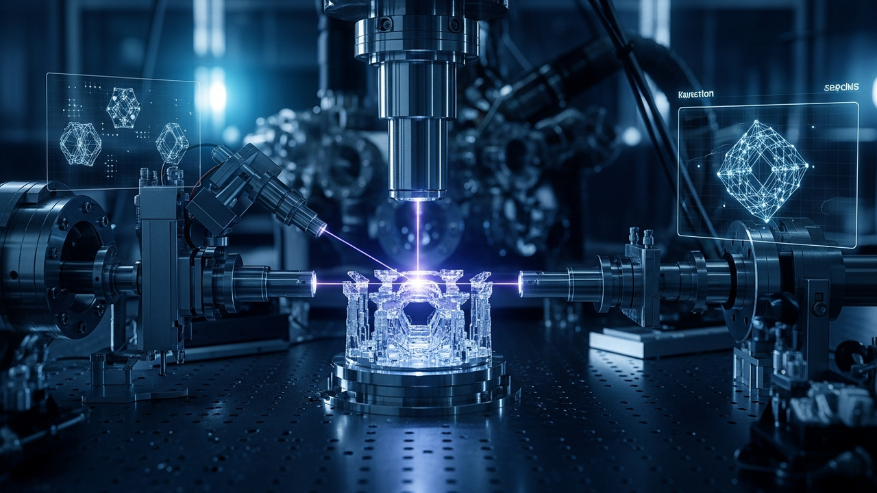
The study involved the direct implantation of krypton ions at specific energies into hBN single-crystal films. This process intentionally introduces stable defect structures, comprising specific vacancies and impurity atoms, into the hBN crystal lattice. A key advantage is the elimination of the high-temperature annealing step typically required to activate or stabilize such defects. Combined temperature-dependent photoluminescence (PL) measurements and electron paramagnetic resonance (EPR) spectroscopy confirmed that the generated defects exhibit stable spin activity at room temperature and possess spectral characteristics indicative of potential quantum bit coherence times. This annealing-free approach simplifies manufacturing and helps mitigate damage to delicate device structures.
Background & Context
Stable, spin-active defects in wide bandgap semiconductors are essential for realizing single-photon sources and spin qubits in quantum information processing, especially quantum photonics. Hexagonal boron nitride (hBN), with its excellent optical properties, high dielectric constant, and 2D structure, has garnered significant attention as a promising quantum material alternative to diamond nitrogen-vacancy (NV) centers. However, controllably generating spin defects in hBN in a manner compatible with integrated circuits has been a major challenge towards practical applications. Traditionally, defect generation often required electron irradiation followed by high-temperature annealing, posing barriers to scalability and manufacturing cost.
Strategic Significance & Outlook
This annealing-free method for generating spin defects via krypton ion implantation paves the way for realizing high-performance quantum sensors, quantum communication devices, and quantum computers based on hBN. The simplification of the manufacturing process directly translates to potential for mass production and cost reduction of hBN quantum devices, accelerating the societal implementation of quantum technologies. The research team is expected to further extend the coherence times of the generated defects and achieve site-selective control of defects within device architectures, anticipating an expanded role for hBN in quantum materials science.
Source: https://arxiv.org/abs/2606.23456
Get our weekly technology intelligence — free
Receive an infographic that lets you judge at a glance whether each field’s analysis report is worth reading.
Subscribe Free — Weekly Tech Intelligence
By subscribing, you’ll receive Troy-Technical’s weekly technology intelligence newsletter.
- Your email and selected fields are used only to deliver the newsletter.
- We never share your information with third parties.
- You can unsubscribe anytime via the link in each email.
See our Privacy Policy for details.
Takes about a minute · Unsubscribe anytime


Comments