Background
The relentless expansion of artificial intelligence (AI) applications has profoundly transformed the semiconductor landscape. For demanding AI workloads requiring immense data processing and high-speed computation, the bandwidth of memory supporting CPUs and GPUs has become as crucial as the processors themselves. High-Bandwidth Memory (HBM) achieves superior data transfer rates by vertically stacking multiple DRAM dies and connecting them through a wide interface to logic chips like GPUs. In the production of HBM, the post-wafer fabrication packaging process is a critical stage that dictates final product performance and yield.
Key Findings / Results
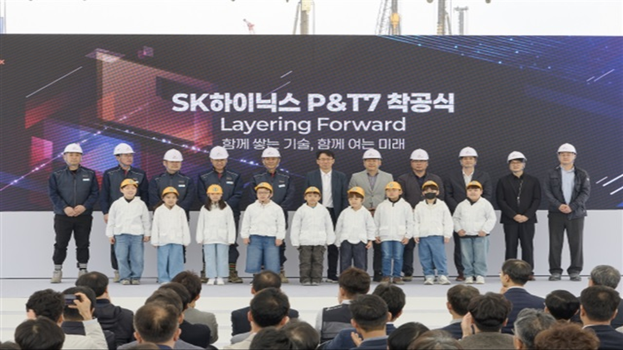
SK Hynix has commenced construction of a new, large-scale advanced packaging facility in Cheongju Technopolis, South Korea, to substantially expand its production capacity for HBM and other AI-centric memory. This investment epitomizes an industry-wide trend where the competitive battleground in AI semiconductors is shifting from leading-edge frontend wafer fabrication to the complexities and performance-determining aspects of back-end advanced packaging technologies. Through this new packaging hub, SK Hynix aims to fortify its HBM stacking, thermal management, and testing capabilities, thereby reinforcing its leadership in the AI memory market. Cheongju is a key manufacturing base for SK Hynix, and the new facility is expected to leverage synergies with existing infrastructure.
Technical Significance & Outlook
The establishment of SK Hynix’s HBM packaging hub in Cheongju holds significant implications for the global AI memory market. In an environment of persistent HBM supply shortages driven by escalating AI demand, this facility will be instrumental in ensuring stable HBM supply and alleviating bottlenecks in AI accelerator production. This enhanced supply could bolster deliveries to major AI chip manufacturers such as Nvidia and AMD, potentially accelerating the growth of the broader AI ecosystem. Furthermore, this investment can be seen as part of a broader “IDM 2.0” strategy, where integrated device manufacturers strengthen their in-house back-end technologies and capacities. Strategic investments in advanced packaging are increasingly becoming a pivotal factor in determining the performance, cost, and time-to-market of future AI semiconductors.
Source: https://www.digitimes.com/news/a20260422VL212/sk-hynix-packaging-hbm-capacity-production.html


Comments