Background
The escalating demands of AI and High-Performance Computing (HPC) are driving rapid advancements in High-Bandwidth Memory (HBM). HBM dramatically increases data transfer speeds by vertically stacking multiple DRAM chips. However, for next-generation HBM4, achieving further performance gains while addressing critical physical challenges like heat dissipation necessitates an evolution beyond traditional microbump bonding. Hybrid bonding, with its finer pitch and superior electrical characteristics, is emerging as the essential technology to meet these stringent requirements.
Key Findings / Results
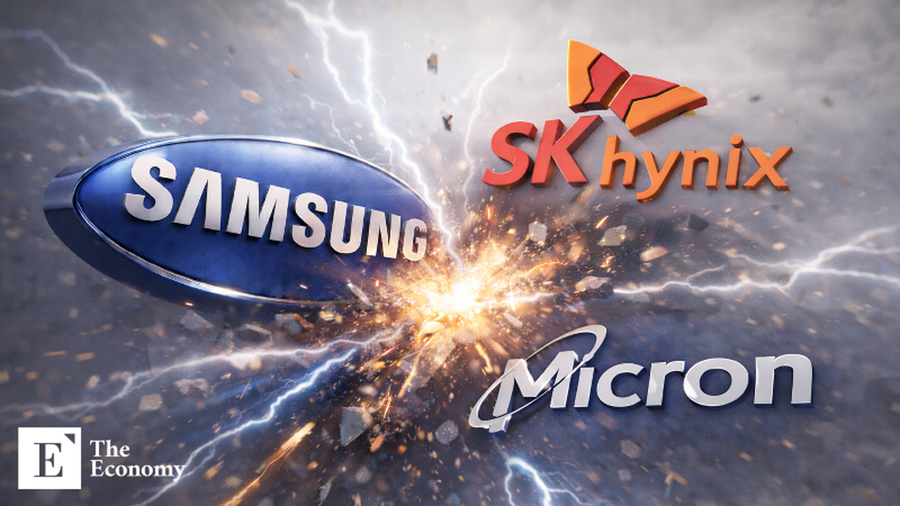
Samsung Electronics has announced the progressive installation of dedicated hybrid bonding lines for HBM4 in its South Korean manufacturing facilities, a strategic move to cement its leadership in the HBM4 market. This technology involves directly bonding DRAM dies and logic dies using copper-to-copper connections, eliminating the need for traditional bumps and significantly reducing the distance between chips. This shortens signal paths, leading to higher data transfer speeds and more effective heat dissipation. Samsung claims to be the first in the world to successfully commence mass production of HBM4 using this hybrid bonding technique, with shipments reportedly already underway to key customers including NVIDIA. Samsung’s HBM4 achieves an operating speed of 11.7Gbps, approximately 46% higher than the JEDEC standard of 8Gbps, with HBM4E potentially reaching data processing speeds from 3.3 TB/s to 4.0 TB/s.
Technical Significance & Outlook
Samsung Electronics’ early adoption of hybrid bonding for HBM4 significantly enhances its competitiveness and technological advantage in the HBM market. This enables Samsung to offer higher-performance and more reliable HBM solutions to AI chip manufacturers like NVIDIA. Competitors such as SK Hynix and Micron are also accelerating their development and deployment of hybrid bonding, intensifying the market share battle for HBM4 and future generations. Hybrid bonding is a pivotal technology for solving the core challenges of the AI semiconductor era—multi-layer HBM stacking, performance enhancement, and thermal management. The progress in its mass production will dictate the pace of evolution for the entire AI ecosystem. This technology’s widespread adoption could ultimately lead to denser 3D integration and establish new standards for semiconductor packaging.


Comments