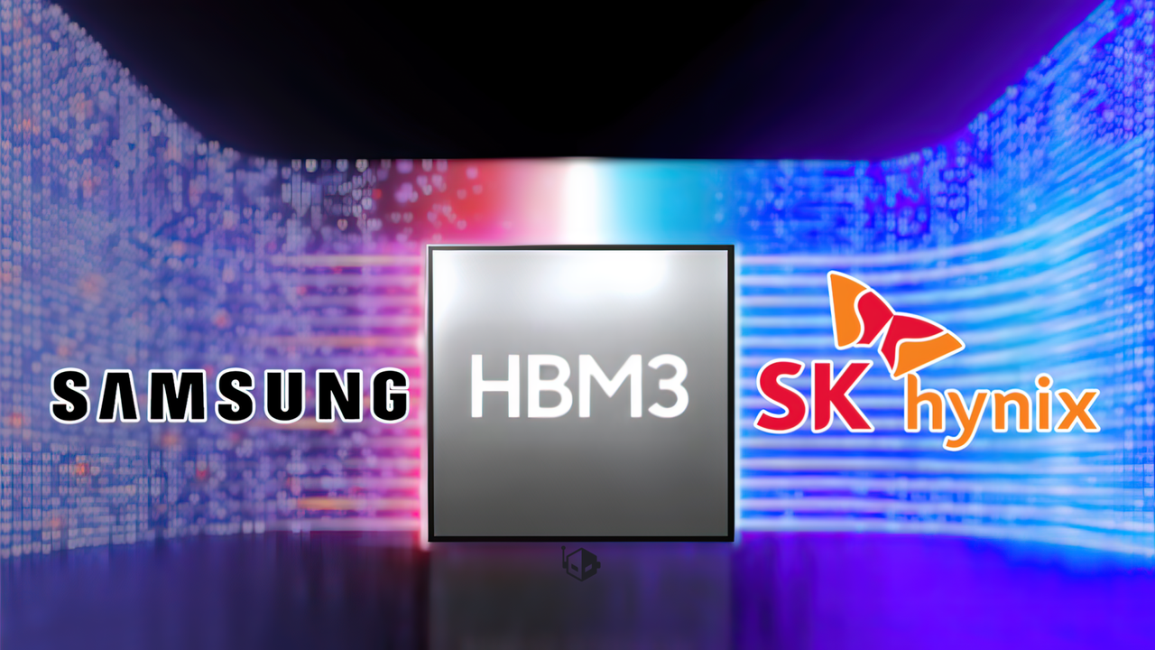
Background
The continuous advancement of artificial intelligence (AI) has positioned High-Bandwidth Memory (HBM) as a critical enabler for high-performance AI accelerators. HBM achieves dramatic improvements in data transfer speeds by vertically stacking multiple DRAM dies. However, next-generation HBM demands even higher layer counts and greater bandwidth, pushing the limits of traditional microbump bonding technologies. Hybrid bonding, with its finer pitch and superior electrical properties, is therefore indispensable. This technology directly connects copper lines between chips, increasing connection density and enhancing signal integrity.
Key Findings / Results
SK Hynix announced significant progress in its hybrid bonding packaging technology for HBM modules. The company has successfully verified a 12-die HBM stack using hybrid bonding, marking a substantial step towards achieving the multi-layer goals for next-generation HBM (HBM4 and HBM5). SK Hynix is currently dedicating efforts to improve the yield of this technology to levels suitable for mass production, although specific yield figures have not been disclosed. Hybrid bonding eliminates the need for traditional bumps by directly joining memory layers, thereby minimizing the distance between chips and contributing to higher data transfer speeds and reduced power consumption. This capability is crucial for accommodating the increasingly fast and complex AI workloads.
Technical Significance & Outlook
SK Hynix’s successful verification of a 12-die HBM stack via hybrid bonding underscores the escalating technological competition in the HBM market. If SK Hynix, a leading HBM supplier, can establish this technology and improve its mass production yield, it will accelerate the market introduction of next-generation AI memory like HBM4 and HBM5, bolstering its market leadership. However, the non-disclosure of specific yield figures suggests that technical challenges persist, particularly concerning cleanliness and thermal management in multi-layer stacks. The commercialization of hybrid bonding will not only impact AI chip performance but also cost efficiency and product reliability. The maturity of this technology is vital for the development of the entire AI hardware ecosystem, and continuous monitoring of HBM market trends remains essential.


Comments