Key Findings
The European Union has approved a substantial €210 million investment under the EU Chips Act to bolster research and development in advanced 3D IC packaging technologies. This move signals a critical commitment to strengthening Europe’s position in the semiconductor value chain and fostering technological autonomy, particularly in back-end manufacturing processes.
Technical / Clinical Details
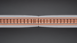
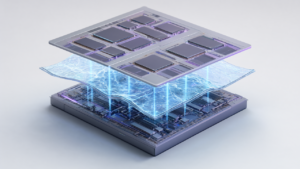
The allocated funds will primarily target projects focused on heterogeneous integration and 3D stacking. These technologies involve combining multiple disparate semiconductor dies and functionalities into a single package, promising significant improvements in performance, power efficiency, and form factor. Research initiatives will encompass advanced interconnect solutions, sophisticated thermal management strategies, and novel chiplet-based design methodologies. The objective is to overcome the limitations of conventional 2D packaging, enabling breakthroughs essential for high-growth sectors such as high-performance computing (HPC), artificial intelligence (AI), automotive, and telecommunications.
Background & Context
As the pace of innovation in front-end wafer fabrication decelerates, advanced packaging has emerged as a crucial driver for semiconductor scaling and performance enhancement, especially for demanding AI and HPC workloads. Historically, Europe has been heavily reliant on Asian manufacturers for both front-end and some back-end processes. The EU Chips Act aims to rebalance this by building a comprehensive domestic semiconductor ecosystem, from design to fabrication and packaging. This investment underscores Europe’s determination to cultivate its own advanced packaging capabilities, reducing supply chain vulnerabilities and increasing its strategic influence globally.
Strategic Significance & Outlook
This €210 million investment is expected to catalyze significant advancements in European semiconductor research institutions and companies. It will facilitate the establishment of pilot lines, accelerate proof-of-concept projects, and strengthen collaboration between academia and industry to rapidly commercialize research outcomes. Long-term, the initiative positions Europe to become a leading player in advanced packaging, contributing to a more resilient and diversified global semiconductor supply chain and reinforcing its standing as a hub for cutting-edge technology innovation.
Source: https://www.chosun.com/english/industry-en/2026/06/25/E5R4RKNI4BH4FJEIOPPSNDCH5Q/
Get our weekly technology intelligence — free
Receive an infographic that lets you judge at a glance whether each field’s analysis report is worth reading.
Subscribe Free — Weekly Tech Intelligence
By subscribing, you’ll receive Troy-Technical’s weekly technology intelligence newsletter.
- Your email and selected fields are used only to deliver the newsletter.
- We never share your information with third parties.
- You can unsubscribe anytime via the link in each email.
See our Privacy Policy for details.
Takes about a minute · Unsubscribe anytime