Key Findings
Intel and TSMC, two pivotal forces in the semiconductor industry, are aggressively championing the adoption and advancement of Panel-Level Packaging (PLP) technology. This concerted effort is projected to expand the associated market by up to tenfold, signaling a significant shift in the landscape of high-performance semiconductor manufacturing, particularly for AI and High-Performance Computing (HPC) chips.
Technical / Clinical Details
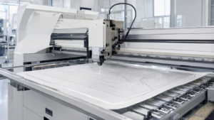
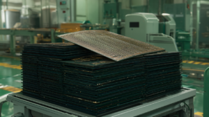
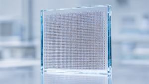
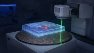
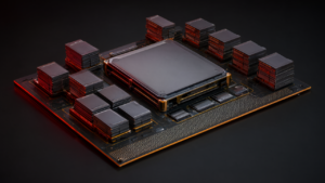
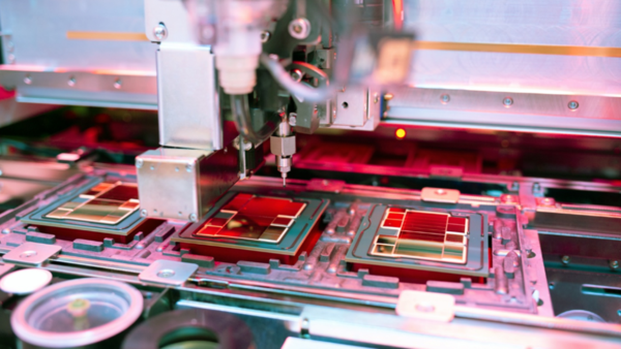
Panel-Level Packaging involves packaging multiple chips simultaneously on larger, rectangular panel substrates instead of traditional round silicon wafers. This methodology significantly improves material utilization and overall throughput by minimizing waste from wafer edge losses. Intel has been actively integrating PLP concepts into its advanced packaging technologies such as ‘Foveros’ and ‘EMIB,’ including Fan-out Panel-Level Packaging (FO-PLP). TSMC, likewise, is exploring PLP as an evolution of its CoWoS (Chip-on-Wafer-on-Substrate) technology, seeking solutions to integrate more chiplets on larger substrates. PLP offers dense interconnection layers and superior thermal dissipation characteristics, making it particularly advantageous for integrating AI processors with High Bandwidth Memory (HBM).
Background & Context
The explosive demand for AI chips has created severe bottlenecks in existing advanced packaging capacities, notably with technologies like CoWoS, which currently limits the speed at which new chips can enter the market. Intel and TSMC’s focus on PLP is a strategic response to mitigate these supply constraints and enable the mass production of high-performance chips in a more cost-effective manner. PLP has the potential to reduce manufacturing costs by 20-30%, which is expected to accelerate the proliferation of high-performance semiconductors not just for AI, but also across a broader range of applications including mobile devices, data centers, and automotive systems. This technological pivot is poised to usher the semiconductor industry into a new phase of growth.
Strategic Significance & Outlook
The aggressive pursuit of PLP by Intel and TSMC represents a paradigm shift in semiconductor manufacturing. As both companies push for the commercialization and mass production of this technology, the entire market for PLP-related equipment, materials, and services is expected to experience substantial growth, creating new business opportunities for equipment manufacturers and material suppliers. In the long term, PLP is anticipated to become one of the mainstream advanced packaging technologies, laying a foundational pillar for the continued evolution of AI and HPC. This innovation will significantly improve the cost-performance balance of next-generation semiconductors, benefiting a wide array of industrial sectors.
Source: https://www.thelec.net/news/articleView.html?idxno=11912
Get our weekly technology intelligence — free
Receive an infographic that lets you judge at a glance whether each field’s analysis report is worth reading.
Subscribe Free — Weekly Tech Intelligence
By subscribing, you’ll receive Troy-Technical’s weekly technology intelligence newsletter.
- Your email and selected fields are used only to deliver the newsletter.
- We never share your information with third parties.
- You can unsubscribe anytime via the link in each email.
See our Privacy Policy for details.
Takes about a minute · Unsubscribe anytime