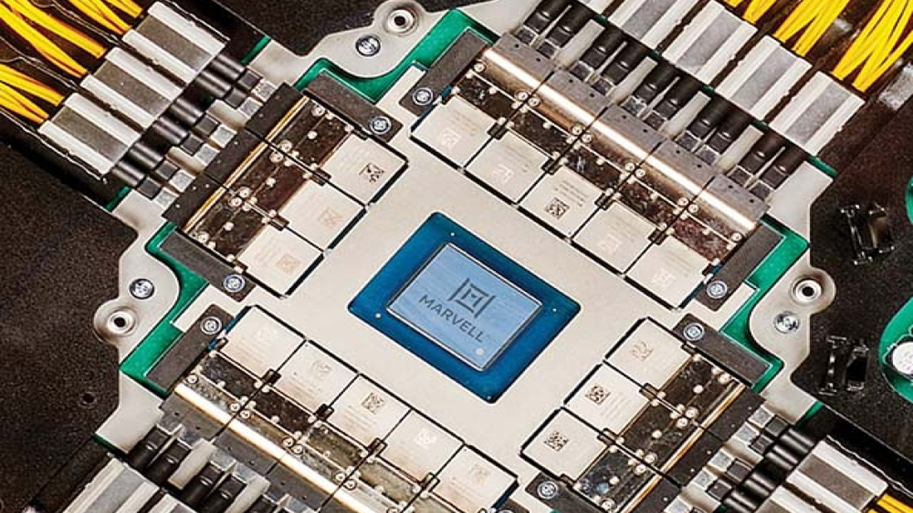
Scale-Up Challenges in AI Infrastructure and the Need for Opticalization
In the era of generative AI, data center performance is determined not just by the capabilities of individual GPUs or ASICs, but by the ability to efficiently coordinate thousands of accelerators in a ‘scale-up’ fashion. This large-scale cooperative operation requires a network that transfers massive amounts of data at ultra-high speed and low latency. However, traditional copper-based electrical links have reached their physical limits in terms of power consumption, signal attenuation, and bandwidth. Consequently, the transition to Co-Packaged Optics (CPO) and Near-Packaged Optics (NPO), which integrate electrical-to-optical conversion very close to the ASIC package, has become an inevitable choice for resolving AI infrastructure performance bottlenecks.
Manufacturing Bottleneck Shifts to ‘Testing’
The transition to CPO/NPO introduces new challenges to the manufacturing process of optical components. While traditional optical module manufacturing primarily relied on testing after final assembly, with CPO, where optical engines are integrated into the ASIC package, the manufacturing bottleneck shifts from conventional assembly processes to ‘optical testing.’ This is because complex devices, with tightly integrated optical and electrical functionalities, need to be efficiently and reliably tested at the mass production scale of the semiconductor industry.
Demand for Scalable Optical Testing and the Importance of DfT
Traditional custom-built, low-volume optical testing methods are inadequate for CPO devices, which feature a high channel count and large production volumes. Therefore, innovative optical testing approaches are urgently required, including:
- High-Parallel Processing and Automation: To efficiently test CPO devices with hundreds to thousands of optical channels, automated optical testing systems capable of high-parallel processing are necessary. This includes wafer-level optical testing and the integration of opto-electronic probe cards.
- Design-for-Test (DfT): Implementing Design-for-Test (DfT) from the design stage is essential. This allows for the identification of Known Good Dies (KGD) early in the manufacturing process, significantly reducing costs associated with integrating defective silicon downstream.
- IC-Style Manufacturing Test Framework: It is necessary to apply established semiconductor manufacturing test expertise to optical testing and build a unified manufacturing test framework.
Impact on Industrialization and Data Center Demand
The widespread adoption of CPO/NPO in AI data centers requires a high-reliability and cost-efficient supply of optical engines, and scalable optical testing technology is key to achieving this. As test technology maturity will determine the pace of industrialization, capital investment in optical test automation and high-parallelization, establishment of DfT-aware design flows, and standardization of optical test technology will be crucial challenges for future industrial development.
Source: https://picmagazine.net/article/124179/Why_scale-up_AI_networks_demand_scalable_optical_test


Comments