Background
For decades, the semiconductor industry has doubled transistor density in accordance with Moore’s Law. However, this pace is slowing due to physical limitations and escalating manufacturing costs. To overcome these challenges, the industry is shifting its focus beyond traditional miniaturization to embrace 3D structuring, the introduction of novel materials, and atomic-level precision control technologies. ALD and ALE serve as foundational pillars supporting these next-generation advancements, being actively adopted and developed by leading semiconductor manufacturers and research institutions worldwide. Their importance is continuously rising, especially with the growing demand for advanced logic, high-performance memory, and devices with new functionalities (e.g., AI chips, IoT devices).
Key Findings
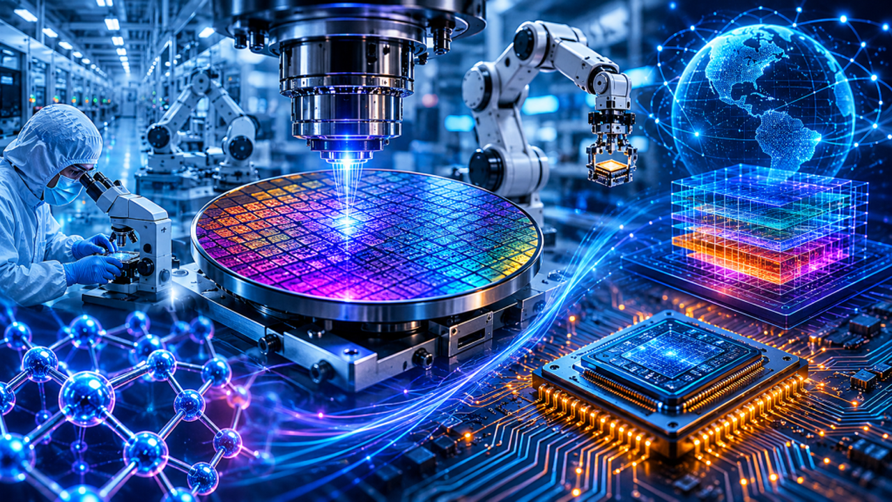
In the realm of semiconductor manufacturing, nanoscale precision processes like Atomic Layer Deposition (ALD) and Atomic Layer Etching (ALE) are increasingly recognized as indispensable core technologies for the miniaturization and performance enhancement of next-generation semiconductor devices. These technologies play a decisive role in transcending the limitations of conventional Moore’s Law, bringing new functionalities and superior performance to semiconductor devices.
Technical Details
ALD is a thin-film deposition technique that leverages self-limiting surface reactions by alternately introducing precursor gases, enabling atomic-layer-level film growth. This process offers exceptional film thickness control, uniformity, and the ability to conformally deposit films onto complex 3D structures. For instance, in next-generation 3D NAND flash memory and FinFET transistors, ALD is crucial for forming uniform insulating and high-k dielectric films within high-aspect-ratio trenches and fin structures. ALE, often considered the inverse process of ALD, selectively removes material one atomic layer at a time. This enables pattern formation with extremely high selectivity and anisotropy (where the vertical etch rate is significantly faster than the lateral rate), achieving precise fabrication of minute circuit structures. By combining these technologies, semiconductor manufacturers can produce a wide variety of high-performance devices, including logic devices at 2nm nodes and below, high-density memory, and power semiconductors. ALD and ALE are also being applied in the research and development of quantum devices and novel materials, facilitating nanoscale material control.
Outlook
The continued evolution of ALD and ALE technologies is indispensable for shaping the future of the semiconductor industry. Future R&D will focus on expanding their applicability to a broader range of materials, enhancing process speed, optimizing cost efficiency, and further reducing defect density. Particular emphasis is expected on technologies enabling the deposition of composite materials and more complex atomic-layer manipulations (e.g., hybrid ALD-CVD processes). These advancements will empower semiconductor devices with enhanced performance and multifunctionality, continuing to provide the foundation for next-generation innovative technologies such as AI, 5G/6G communication, autonomous driving, and quantum computing. ALD and ALE are poised to carve out new frontiers for sustainable growth and technological innovation in the semiconductor industry.
Source: https://www.eletimes.ai/advances-in-core-technologies-for-semiconductor-manufacturing


Comments