Key Findings
A groundbreaking research paper reports the successful and highly precise control of the quantum confinement effect in heteromorphic PbS/SnS2 superlattices fabricated using Atomic Layer Deposition (ALD). This study establishes ALD as an exceptionally effective platform for quantum superlattice engineering in complex chalcogenide heterostructures, opening critical avenues for the development of next-generation optoelectronic and quantum devices. Specifically, the researchers demonstrated a systematic and controllable expansion of the material’s bandgap from 1.74 eV to 2.51 eV by progressively decreasing the thickness of the PbS sublayers.
Technical and Clinical Details
The quantum confinement effect describes the alteration of a semiconductor material’s electronic structure and the expansion of its bandgap as its size approaches the de Broglie wavelength of electrons. Controlling this effect is paramount for tailoring the properties of optoelectronic devices such as photodetectors, solar cells, LEDs, and lasers.
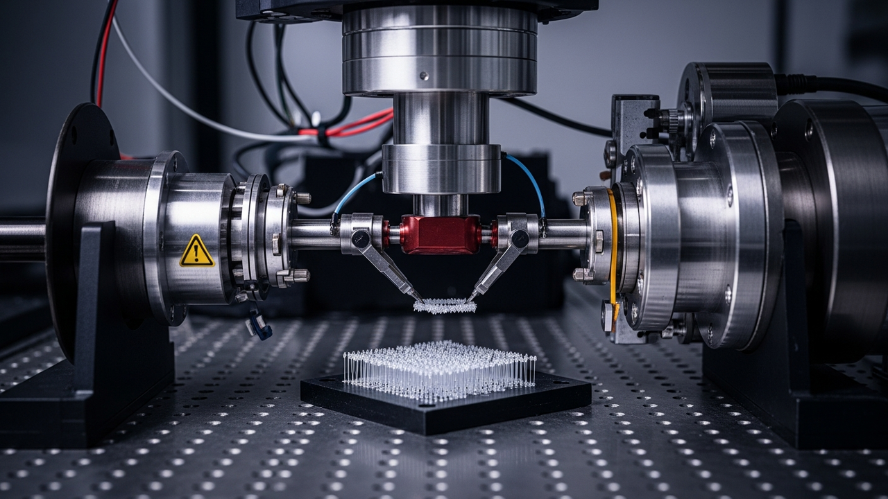
In this research, the atomic-level thickness control capability of ALD was fully leveraged to construct high-quality superlattice structures by alternately depositing layers of PbS and SnS2, two different semiconductor materials. Critically, ALD’s precise process control enabled the rigorous adjustment of the PbS sublayer thickness at the nanometer scale, which in turn allowed systematic control over the overall quantum confinement effect within the superlattice. Experimentally, it was shown that as the PbS sublayer thinned, the quantum confinement effect intensified, leading to a continuous and predictable increase in bandgap energy from 1.74 eV to 2.51 eV. This wide-ranging bandgap tunability facilitates the design of devices capable of responding to diverse wavelength ranges.
Background and Industry Context
The optoelectronic device sector constantly demands higher performance and multi-functionality, with the development of materials offering freely tunable bandgaps being a long-standing challenge. Traditional semiconductor manufacturing techniques struggled with such atomic-level structural control, preventing the full exploitation of the quantum confinement effect. ALD technology, with its superior uniformity, conformality, and atomic-level thickness control in thin film deposition, has been increasingly recognized for its importance in fabricating complex nanostructures and heterostructures.
Strategic Significance and Outlook
This technology, which precisely controls the quantum confinement effect in heteromorphic PbS/SnS2 superlattices using ALD, is poised to have a significant impact on the development of next-generation high-performance optoelectronic and quantum devices. Broad applications are anticipated, including highly efficient solar cells, sensitive infrared detectors, efficient light-emitting devices, and quantum dot devices tailored for specific wavelengths. This research underscores that ALD is not merely a thin-film deposition tool but a powerful platform in quantum materials engineering, and it is expected to accelerate further innovation in this field.
Source: https://pubmed.ncbi.nlm.nih.gov/
Get our weekly technology intelligence — free
Receive an infographic that lets you judge at a glance whether each field’s analysis report is worth reading.
Subscribe Free — Weekly Tech Intelligence
By subscribing, you’ll receive Troy-Technical’s weekly technology intelligence newsletter.
- Your email and selected fields are used only to deliver the newsletter.
- We never share your information with third parties.
- You can unsubscribe anytime via the link in each email.
See our Privacy Policy for details.
Takes about a minute · Unsubscribe anytime


Comments