Key Findings
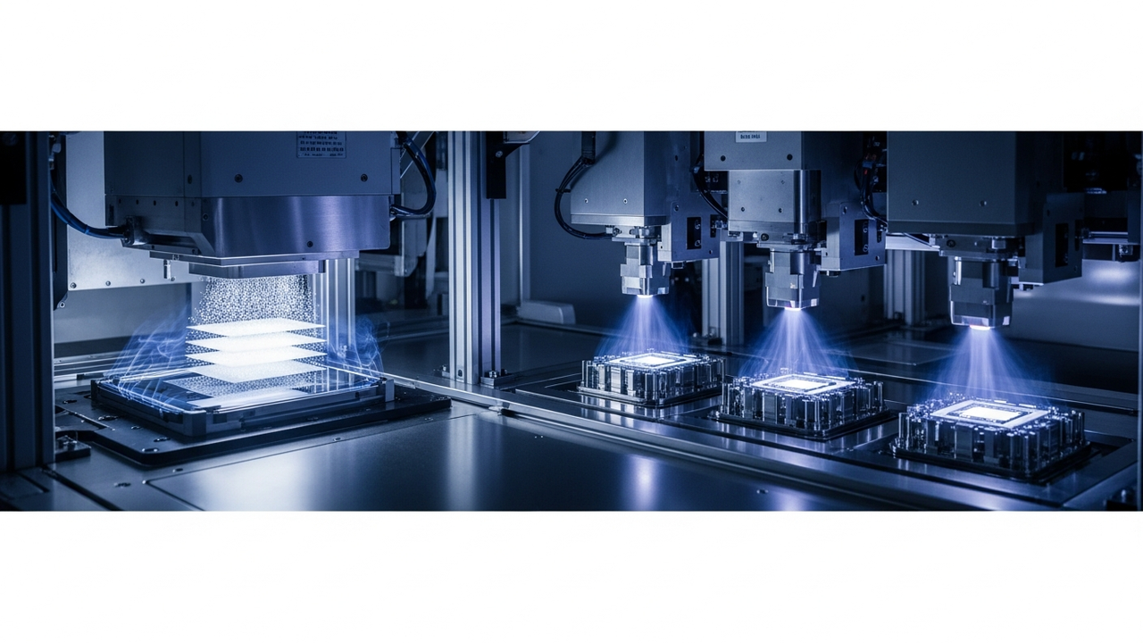
Applied Materials, a leading semiconductor equipment manufacturer, has unveiled innovative new deposition and selective etch systems designed to further advance 3D chip scaling technology. The new offerings include the Centris Spectral SiN ALD (Atomic Layer Deposition) system, capable of depositing uniform, low-temperature silicon nitride in high-aspect-ratio 3D structures. This technology is particularly critical for forming contact liners in Gate-All-Around (GAA) transistors and has already been adopted by major chipmakers.
Technical and Clinical Details
The Centris Spectral SiN ALD system is engineered to form silicon nitride (SiN) films with uniform thickness and excellent conformality within complex 3D structures, such as around the nanosheet channels of GAA transistors, at low process temperatures. Conventional deposition techniques struggle to form uniform films at the bottom and sidewalls of high-aspect-ratio structures, which has been a bottleneck for device performance and reliability. The low-temperature process mitigates the risk of thermal damage to delicate 3D structures and enhances compatibility with existing materials.
This SiN film functions as a contact liner, providing electrical isolation between the gate electrode and the channel in GAA transistors. The uniform deposition of SiN in high-aspect-ratio configurations directly leads to improved GAA transistor performance, reduced leakage current, and enhanced yield. Applied Materials’ new selective etch systems are designed to precisely remove unwanted materials from these intricate 3D structures, enabling further miniaturization and vertical integration in next-generation chips.
Background and Industry Context
The semiconductor industry is facing the limits of planar scaling as it pursues ever-greater performance and miniaturization of integrated circuits. To overcome this challenge, “3D chip scaling” technologies, such as GAA transistors and 3D NAND flash memory, have become indispensable. These technologies require complex high-aspect-ratio structures, demanding atomic-level precision in deposition and etching during manufacturing. Applied Materials’ new systems address these cutting-edge process requirements, forming foundational technologies for the future semiconductor roadmap.
Strategic Significance and Outlook
Applied Materials’ new deposition and selective etch systems are set to significantly improve the manufacturability of next-generation chips in logic and memory applications, thereby boosting device performance. Early adoption by leading chipmakers underscores the critical necessity of this technology for the industry. As these technologies become more widely implemented, they are expected to accelerate the development of more powerful and energy-efficient AI processors, high-performance mobile devices, and data center chips. This represents a crucial investment for sustaining continuous innovation and technological leadership in the semiconductor industry, demonstrating how nanotechnology underpins modern electronics.
Get our weekly technology intelligence — free
Receive an infographic that lets you judge at a glance whether each field’s analysis report is worth reading.
Subscribe Free — Weekly Tech Intelligence
By subscribing, you’ll receive Troy-Technical’s weekly technology intelligence newsletter.
- Your email and selected fields are used only to deliver the newsletter.
- We never share your information with third parties.
- You can unsubscribe anytime via the link in each email.
See our Privacy Policy for details.
Takes about a minute · Unsubscribe anytime

Comments