Background
The semiconductor industry is rapidly transitioning towards 3D integration technologies, moving beyond traditional 2D scaling as it confronts the physical limits of Moore’s Law. Hybrid bonding is a pivotal technology that precisely joins different wafers to improve chip performance, power efficiency, and functional density. Furthermore, quantum computing, with its potential to solve complex problems intractable for classical computers, is attracting significant investment from governments and major corporations globally. EVG’s technological advancements provide a critical foundation supporting manufacturing capabilities and innovation in these cutting-edge fields.
Key Findings
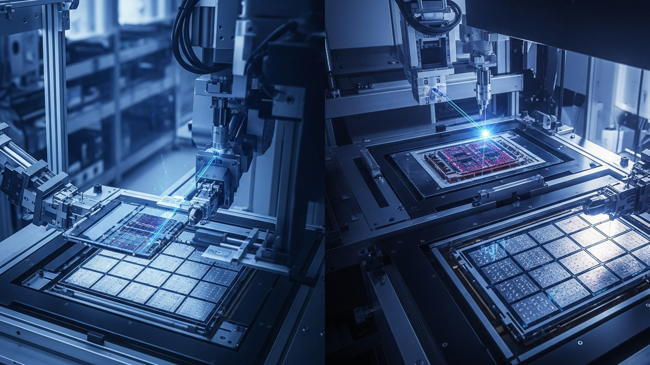
EV Group (EVG) has achieved a significant technical milestone in advanced wafer-to-wafer hybrid bonding, demonstrating 200nm pitch with a high-precision overlay accuracy of less than 40nm, a feat accomplished in collaboration with imec. This breakthrough significantly expands the possibilities for 3D integration in semiconductor manufacturing. Simultaneously, EVG has signed a Memorandum of Understanding (MoU) with Silicon Austria Labs (SAL) aimed at scaling quantum technologies, thereby accelerating its global manufacturing and partnership strategy in the quantum computing sector.
- Hybrid Bonding Advancement: EVG and imec have successfully demonstrated wafer-to-wafer hybrid bonding at a 200nm pitch, achieving an impressive overlay accuracy of less than 40nm. This technology is critical for significantly increasing transistor density and enabling highly reliable, high-performance interconnections in 3D stacked chip manufacturing. Compared to conventional bonding methods, this advancement facilitates finer wiring and higher integration, forming a foundational element for next-generation high-performance logic and memory devices.
- Quantum Technology Scaling Partnership: EVG’s MoU with Silicon Austria Labs (SAL), a leading Austrian research institution, focuses on scaling quantum technologies. This partnership aims to address manufacturing process and scalability challenges inherent in quantum computing, quantum sensors, and other related applications. By combining EVG’s precision wafer processing technology with SAL’s expertise in quantum research, the collaboration is expected to accelerate the commercialization path for quantum devices.
These technical milestones and strategic partnerships are crucial for solidifying EVG’s leadership in the semiconductor and quantum technology sectors. The progress in hybrid bonding will profoundly impact the design and manufacturing of future high-performance semiconductor chips, driving innovation in markets such as AI, high-performance computing (HPC), and mobile devices. The quantum technology collaboration is expected to accelerate the practical application of quantum computing, positioning it as a long-term growth driver for the company. EVG plans to continue focusing on solving technical challenges and promoting commercialization in these areas through ongoing collaboration with its partners.
Source: https://www.distillintelligence.com/news/ev-group
Get our weekly technology intelligence — free
Receive an infographic that lets you judge at a glance whether each field’s analysis report is worth reading.
Subscribe Free — Weekly Tech Intelligence
By subscribing, you’ll receive Troy-Technical’s weekly technology intelligence newsletter.
- Your email and selected fields are used only to deliver the newsletter.
- We never share your information with third parties.
- You can unsubscribe anytime via the link in each email.
See our Privacy Policy for details.
Takes about a minute · Unsubscribe anytime

Comments