Key Findings
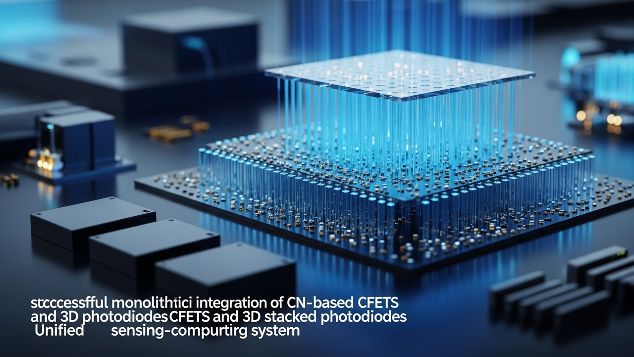
The first successful monolithic integration of carbon nanotube (CNT)-based complementary field-effect transistors (CFETs) with 3D-stacked photodiodes has been achieved. This innovative system capitalizes on CNTs’ exceptional electrical and optoelectronic properties, combined with their low-temperature processability, to offer a highly promising material platform for M3D integration. This platform unifies digital logic and functional sensing elements on a single chip, paving the way for next-generation integrated systems that seamlessly link sensing and computing.
Technical / Clinical Details
In this study, a true CFET architecture utilizing CNTs as channel materials was implemented. CFETs, which stack n-type and p-type transistors vertically or horizontally, achieve both high drive current and low leakage current, offering advantages in reduced power consumption and footprint compared to traditional CMOS technology. This CNT-based CFET is 3D-stacked with silicon-based photodiodes, functioning as a ‘unified sensing and computing system’ that processes everything from optical signal detection to digital computation. The low-temperature process compatibility of CNTs plays a crucial role in enabling multi-layer device stacking while maintaining compatibility with existing semiconductor manufacturing techniques, thereby achieving high-density integration.
Background & Context
Modern electronic devices demand smaller footprints, higher functionality, and lower power consumption. Particularly with the advancement of artificial intelligence (AI) and IoT devices, there’s a growing need for ‘intelligent sensors’ that integrate sensors and processors to efficiently handle data collection and processing. However, traditional silicon-based technologies faced limitations in physically integrating digital circuits with optical sensors while maintaining performance. CNTs, owing to their unique properties (high mobility, tunable bandgap, excellent photoresponsivity), hold the potential to overcome these challenges and have been recognized as a promising platform for next-generation ‘monolithic 3D (M3D) integration.’
Strategic Significance & Outlook
The monolithic integration of CNT-based CFETs with 3D-stacked photodiodes holds the potential to revolutionize diverse application fields, including wearable devices, smart sensors, image recognition systems, and even neuromorphic computing. Specifically, it is expected to enable ‘in-sensor computing’ for edge AI devices, allowing for high-speed, on-the-spot processing of sensor data and real-time decision-making. This technology is poised to dramatically enhance information processing efficiency and significantly reduce power consumption, contributing to a more sustainable and intelligent society. Further advancements in integration density and optimization of manufacturing processes will undoubtedly lead to the creation of new markets.
Source: https://pubs.acs.org/doi/10.1021/acsnano.6c04995
Get our weekly technology intelligence — free
Receive an infographic that lets you judge at a glance whether each field’s analysis report is worth reading.
Subscribe Free — Weekly Tech Intelligence
By subscribing, you’ll receive Troy-Technical’s weekly technology intelligence newsletter.
- Your email and selected fields are used only to deliver the newsletter.
- We never share your information with third parties.
- You can unsubscribe anytime via the link in each email.
See our Privacy Policy for details.
Takes about a minute · Unsubscribe anytime


Comments