Background and Industry Context
The semiconductor industry has been characterized by a relentless pursuit of miniaturization and performance enhancement, famously encapsulated by Moore’s Law. However, with increasingly complex device architectures and the proliferation of new materials, controlling manufacturing processes and ensuring quality have become progressively more challenging. When a manufactured device’s performance deviates from design targets, accurately solving the inverse problem – pinpointing the root cause by tracing back to underlying material properties – is crucial for rapid yield improvement and cost reduction. Traditionally, inverse problem analysis relied either on expert empirical judgment or computationally intensive simulation and optimization methods, both of which are prohibitively slow for real-time application.
Key Findings
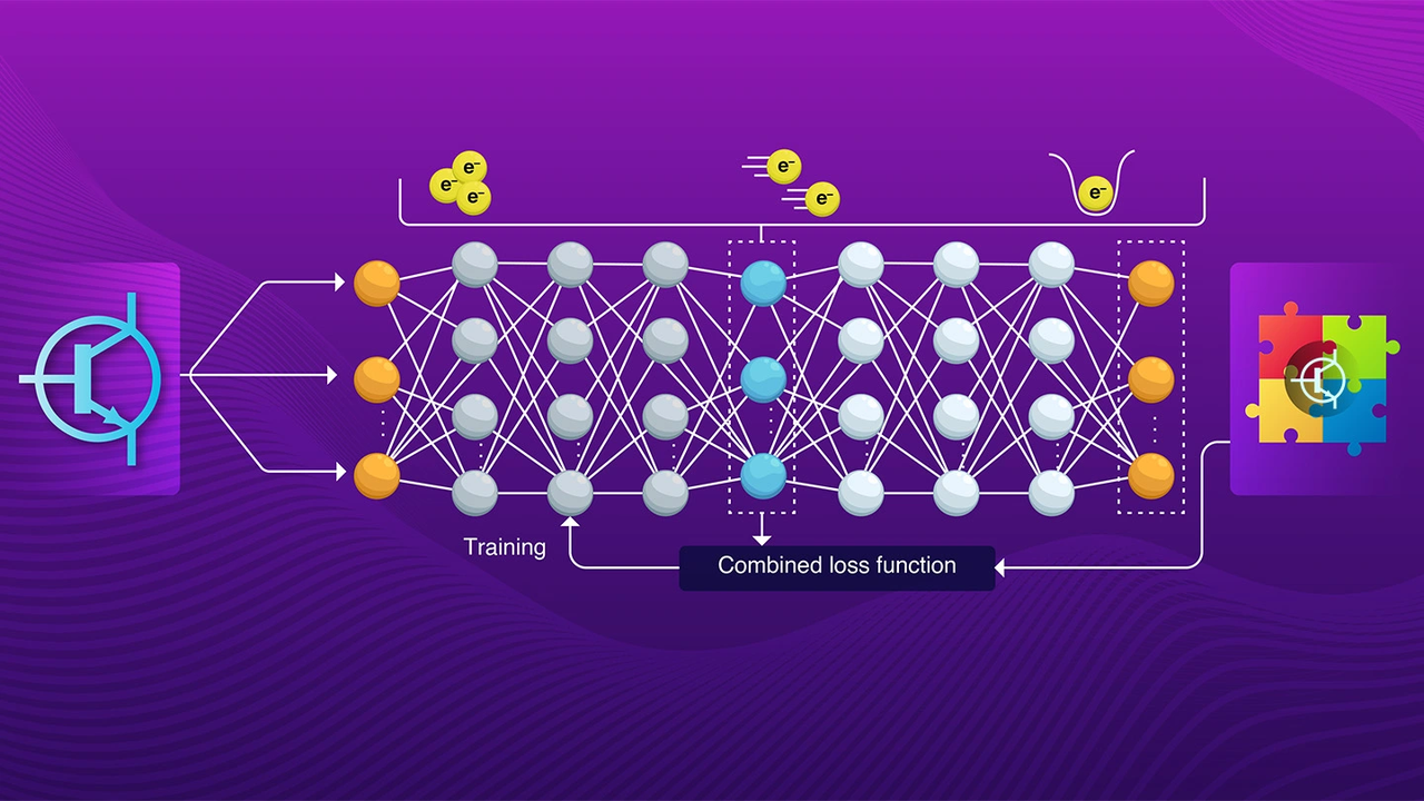
A research team at the Tokyo Institute of Science has developed a tandem neural network that solves the long-standing ‘inverse problem’ in semiconductor device analysis with unprecedented speed. This AI system can accurately infer critical physical parameters of semiconductor materials, such as impurity concentration, carrier mobility, and film thickness, directly from standard transistor electrical measurements in less than one millisecond. This enables real-time execution of complex analyses that previously required hours or even days, delivering transformative efficiency gains for semiconductor R&D and manufacturing.
Technical Details
The inverse problem in semiconductor devices involves inferring the microscopic properties of constituent materials from externally measurable electrical signals, such as forward voltage or current-voltage (I-V) characteristics. This problem is notoriously challenging due to its inherent ‘multi-valuedness,’ where multiple distinct sets of physical parameters can yield similar electrical responses. The tandem neural network developed by the Tokyo Institute of Science employs a novel architecture comprising two cascaded neural networks specifically designed to overcome this multi-valuedness. The first network generates a diverse set of potential material parameter candidates from the input measurements, while the second network acts as a discriminator and refiner, selecting the most physically plausible solution.
This innovative architecture grants the AI system high reliability in solving complex inverse problems. Extensive experimental validation, conducted by training the system on virtual devices with diverse transistor structures and material parameters, demonstrated its capability to accurately estimate physical parameters within a few percentage points of error, even under realistic noisy measurement conditions. This sub-millisecond response time offers a decisive advantage for crucial applications like inline quality control in modern semiconductor manufacturing lines and accelerating the autonomization of materials development.
Future Outlook
This tandem neural network is poised to trigger significant transformations in R&D and manufacturing processes across the semiconductor industry. Moving forward, the technology is expected to extend its application to a broader spectrum of semiconductor devices, including high-power devices and optoelectronics, as well as emerging materials such as wide-bandgap semiconductors and 2D materials. Furthermore, integrating this AI system into automated process control systems or ‘self-driving labs’ will lay the groundwork for fully autonomous semiconductor material development and manufacturing cycles. Ultimately, by drastically shortening semiconductor device design cycles, reducing manufacturing costs, and improving product quality and reliability, this technology is projected to accelerate the advancement of critical next-generation fields such as AI/IoT, 5G/6G communication, and quantum computing.
Source: https://www.isct.ac.jp/en/news/tky57fxj4rub
Get our weekly technology intelligence — free
Receive an infographic that lets you judge at a glance whether each field’s analysis report is worth reading.
Subscribe Free — Weekly Tech Intelligence
By subscribing, you’ll receive Troy-Technical’s weekly technology intelligence newsletter.
- Your email and selected fields are used only to deliver the newsletter.
- We never share your information with third parties.
- You can unsubscribe anytime via the link in each email.
See our Privacy Policy for details.
Takes about a minute · Unsubscribe anytime


Comments