Key Findings
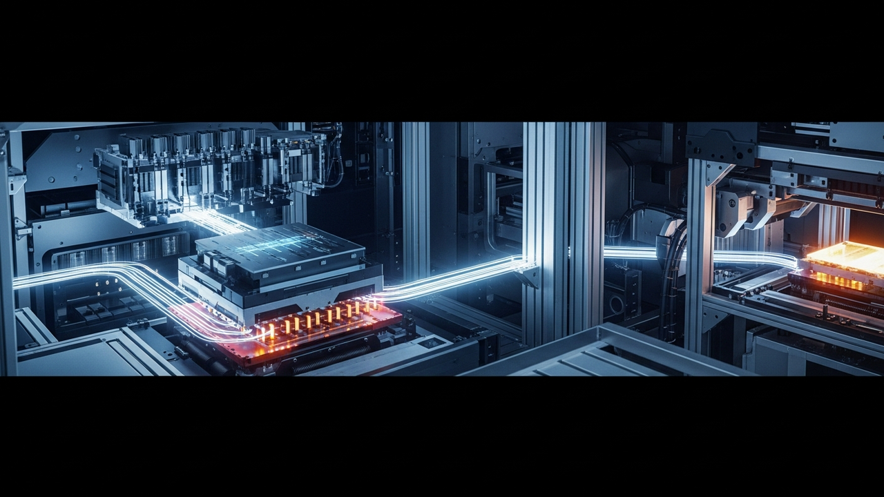
Applied Materials has unveiled a new lineup of material engineering systems engineered to significantly accelerate the production of advanced 3D chip architectures, which are critical enablers for next-generation artificial intelligence (AI). These systems are specifically designed to enhance yield and performance in critical processes such as High Bandwidth Memory (HBM) and logic chip vertical stacking.
Technical Details
The newly introduced systems incorporate several key technologies:
- Advanced Chemical Mechanical Planarization (CMP) Systems: These systems are crucial for achieving ultra-flat surfaces during HBM and logic chip stacking, which dramatically improves the reliability of electrical connections between stacked layers. This precision is paramount for boosting the yield rates of complex 3D stacking processes.
- High-Performance Deposition Systems: Capable of forming ultra-thin and highly uniform layers, these systems optimize interconnect performance and minimize signal propagation delays. Their role is particularly vital in the Through-Silicon Via (TSV) processes essential for advanced HBM modules.
- eBeam Defect Review Systems: Providing high-speed and high-accuracy detection of minute defects within intricate advanced packaging structures, these systems are key to enhancing product reliability and reducing manufacturing costs in high-volume production environments.
These technological advancements offer foundational solutions for overcoming the limitations of traditional 2D scaling, enabling the practical implementation of 3D integration. As AI applications demand ever-increasing data processing capabilities and lower power consumption, the evolution of HBM and chiplet technologies becomes indispensable, and Applied Materials’ new systems directly address these emerging challenges.
Background & Context
The explosive growth of AI has led to an unprecedented demand for computational power in data centers and edge devices. consequently, advanced packaging technologies that offer high-bandwidth, low-latency memory integration and efficient multi-chip integration have become paramount for the semiconductor industry. Leveraging its extensive expertise in material engineering, Applied Materials aims to solidify its position within the AI semiconductor supply chain by meeting these evolving market requirements.
Strategic Significance & Outlook
Applied Materials anticipates that these new systems will alleviate critical bottlenecks in AI chip design and manufacturing, accelerating the market introduction of more powerful and energy-efficient AI processors. This technological breakthrough is expected to significantly bolster the overall competitiveness of the semiconductor industry in rapidly expanding sectors such as AI, High-Performance Computing (HPC), and data centers.
Get our weekly technology intelligence — free
Receive an infographic that lets you judge at a glance whether each field’s analysis report is worth reading.
Subscribe Free — Weekly Tech Intelligence
By subscribing, you’ll receive Troy-Technical’s weekly technology intelligence newsletter.
- Your email and selected fields are used only to deliver the newsletter.
- We never share your information with third parties.
- You can unsubscribe anytime via the link in each email.
See our Privacy Policy for details.
Takes about a minute · Unsubscribe anytime


Comments