Key Findings
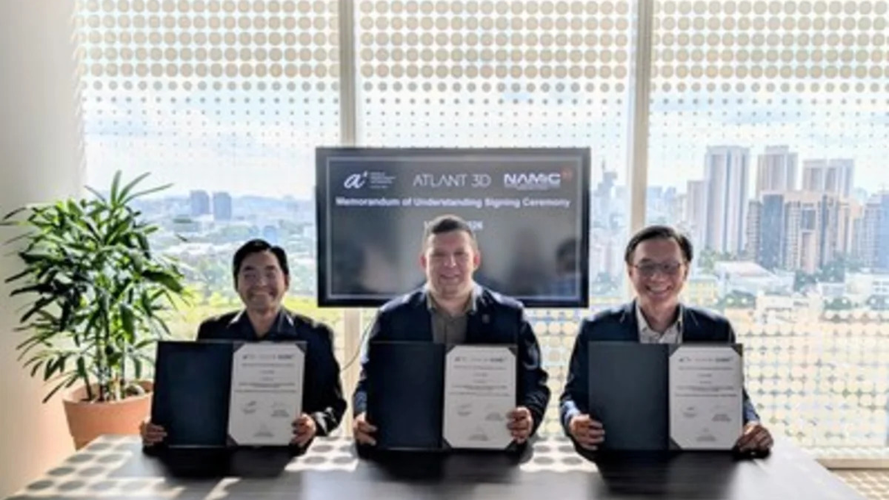
ATLANT 3D, the Agency for Science, Technology and Research’s Institute of Materials Research and Engineering (A*STAR IMRE), and the National Additive Manufacturing Innovation Cluster (NAMIC) have formalized a Memorandum of Understanding to establish a groundbreaking Advanced Materials Development Hub (A-HUB) in Singapore. This strategic collaboration aims to integrate ATLANT 3D’s patented Direct Atomic Layer Processing (DALP®) technology with A*STAR IMRE’s extensive materials science expertise. The core objective is to accelerate innovation in crucial sectors such as semiconductors, silicon photonics, and advanced packaging through AI-driven materials discovery approaches.
Technical / Clinical Details
The A-HUB is designed to fundamentally transform traditional materials discovery processes. Conventional trial-and-error methods are time-consuming and costly, whereas AI-driven methodologies combine vast data analysis and simulation to dramatically accelerate the prediction of new material properties and optimization of synthesis conditions. The key technological components of this hub include:
- Direct Atomic Layer Processing (DALP®): Developed by ATLANT 3D, this technology enables precise, atomic-layer control over material deposition at the nanoscale. This capability facilitates the creation of extremely thin, uniform films and complex 3D structures, contributing to enhanced semiconductor device performance, optimized optical components in silicon photonics, and high-density interconnects in advanced packaging.
- AI-Driven Materials Discovery Platform: Utilizes machine learning algorithms and data science to analyze relationships between material composition, structure, and properties. This accelerates the identification of novel material candidates that meet specific application requirements and optimizes experimental design, thereby shortening R&D cycles.
- High-Throughput Materials Synthesis: Incorporates automated systems and robotics to synthesize and characterize numerous material samples concurrently, speeding up the discovery process.
By integrating these technologies, A-HUB will enable the development of new materials that enhance performance parameters such as power efficiency, data transfer rates, and reliability in semiconductor devices, particularly supporting the evolution of advanced packaging like HBM and chiplets.
Background & Context
The semiconductor industry, confronting the limits of Moore’s Law, is increasingly turning to materials science and advanced packaging as new frontiers for performance enhancement. As demand for AI and High-Performance Computing (HPC) accelerates, challenges related to thermal management, electrical performance, and reliability—which existing materials struggle to address—have become prominent. The discovery and development of new materials are thus key to enabling next-generation semiconductor technologies. Singapore, with its advanced research infrastructure and robust ecosystem, actively invests in R&D for advanced manufacturing and materials science, and this partnership is a part of that strategy.
A*STAR IMRE is a global leader in materials research, and NAMIC is an organization dedicated to driving innovation in additive manufacturing. The collaboration with ATLANT 3D brings together the expertise and cutting-edge technologies of these entities, holding the potential to contribute to global problem-solving in the materials domain.
Strategic Significance & Outlook
The establishment of A-HUB in Singapore is set to maximize the potential of AI-driven materials discovery, dramatically accelerating innovation in the semiconductor, silicon photonics, and advanced packaging sectors. Its capabilities in high-throughput material synthesis and autonomous discovery are expected to significantly reduce the lead time for new material development, thereby expediting market introduction.
For researchers and engineers, this presents an unparalleled opportunity to engage in cutting-edge R&D at the intersection of atomic layer precision processing and AI-powered materials science. For investors, given that advanced materials technology underpins the growth of the AI-era semiconductor industry, investments in this sector are highly attractive from a long-term perspective. The success of A-HUB will not only establish Singapore as a global hub for advanced materials research but also provide a new model for contributing to technological innovation in the global semiconductor industry.
Source: https://sg.finance.yahoo.com/news/atlant-3d-star-imre-namic-073000539.html
Get our weekly technology intelligence — free
Receive an infographic that lets you judge at a glance whether each field’s analysis report is worth reading.
Subscribe Free — Weekly Tech Intelligence
By subscribing, you’ll receive Troy-Technical’s weekly technology intelligence newsletter.
- Your email and selected fields are used only to deliver the newsletter.
- We never share your information with third parties.
- You can unsubscribe anytime via the link in each email.
See our Privacy Policy for details.
Takes about a minute · Unsubscribe anytime


Comments