Key Findings
The European Commission has unveiled the first major project to receive funding under the EU Chips Act, allocating a total of €210 million (approximately $225 million USD) to German semiconductor giant Infineon, a subsidiary of Dutch semiconductor equipment leader ASML, and French materials manufacturer Soitec. This significant investment is specifically targeted at the development of next-generation 3D IC heterogeneous integration and advanced packaging technologies.
Technical Details
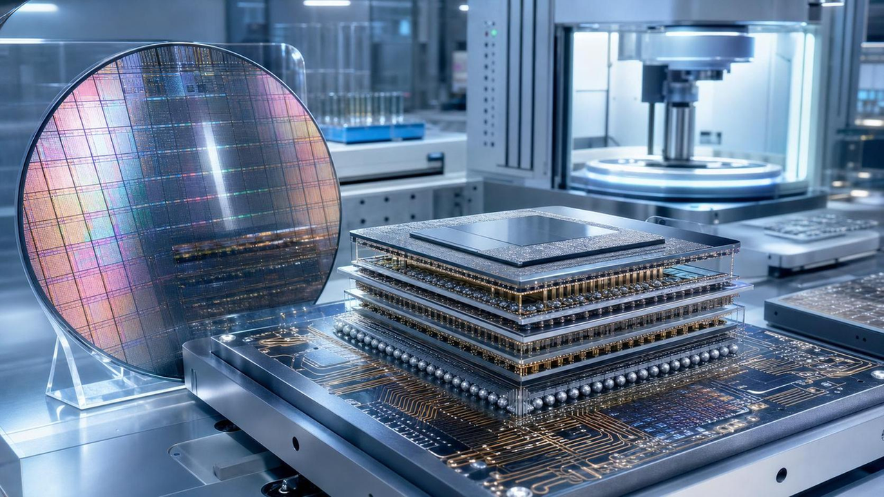
- Funding Allocation: The grants will be utilized for research and development aimed at achieving highly efficient and high-performance 3D IC architectures. This includes technologies for vertically or horizontally integrating multiple chips (e.g., processors, memory, sensors) within a single package.
- Heterogeneous Integration: This technology seeks to enhance system performance, reduce power consumption, and optimize manufacturing costs by combining chiplets produced using different fabrication processes. Specific advancements include heterogeneous integration using Fan-Out Wafer-Level Packaging (FOWLP) for GaN and Si chiplets, and the development of reliable interconnection technologies utilizing electrolytic indium bumps.
- Access Requirements: A key condition of this project is that the technologies developed must be made available to certified suppliers within the EU. This mandate is part of the EU’s broader strategy to enhance the competitiveness of its entire semiconductor supply chain and ensure technological autonomy in critical areas.
Background & Industry Context
The EU Chips Act is a massive initiative, committing €43 billion in public and private investment by 2030, aimed at strengthening Europe’s position in the global semiconductor supply chain and safeguarding against geopolitical risks. With the escalating demand for AI and High-Performance Computing (HPC), advanced packaging has emerged as a primary means to improve system performance as transistor scaling approaches its physical limits. This funding represents a crucial step in bolstering Europe’s technological foundation and fostering innovation in this vital sector.
Strategic Significance & Outlook
This substantial financial injection is expected to generate new business opportunities within the European semiconductor ecosystem, particularly for IC packaging material and advanced substrate suppliers. Infineon, the ASML subsidiary, and Soitec will lead this project, forming a cornerstone for Europe to enhance its presence as a significant player in the global semiconductor race. The technologies developed are anticipated to contribute to next-generation electronic devices across various sectors, including data centers, automotive, and industrial IoT, thereby accelerating the overall digitalization of the European economy.
Get our weekly technology intelligence — free
Receive an infographic that lets you judge at a glance whether each field’s analysis report is worth reading.
Subscribe Free — Weekly Tech Intelligence
By subscribing, you’ll receive Troy-Technical’s weekly technology intelligence newsletter.
- Your email and selected fields are used only to deliver the newsletter.
- We never share your information with third parties.
- You can unsubscribe anytime via the link in each email.
See our Privacy Policy for details.
Takes about a minute · Unsubscribe anytime