Key Findings
Lam Research, a leading supplier of semiconductor manufacturing equipment, is proactively shaping the future of advanced packaging by expanding its wafer-to-panel processing technologies. The company has developed new platforms and processes that enable simultaneous processing of multiple chips on larger panel substrates, delivering dramatic reductions in manufacturing costs and significant improvements in production throughput.
Technical / Clinical Details
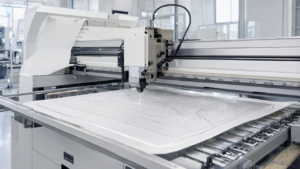
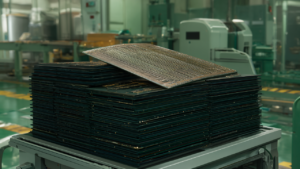
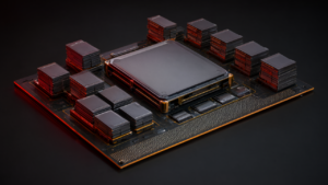
Lam Research’s ‘wafer-to-panel’ strategy focuses on executing advanced packaging processes on large, rectangular panels rather than traditional round wafers. This approach minimizes material waste typically generated at wafer edges, maximizing raw material utilization efficiency. Specifically, the company’s new platforms are designed to perform high-precision etching, thin-film deposition, and cleaning processes at the panel level. This enables the processing of a greater number of chips at once, especially for technologies like Fan-Out Panel-Level Packaging (FOPLP), substantially reducing the cost per unit chip. This technology addresses the increasingly complex demands of next-generation semiconductors, including AI processors, High Bandwidth Memory (HBM), and chiplet integration.
Background & Context
The rapid advancements in artificial intelligence (AI) and high-performance computing (HPC) are posing new challenges to traditional semiconductor manufacturing technologies. Advanced packaging, in particular, is becoming an indispensable factor in determining chip performance, power consumption, and cost. However, existing wafer-level packaging technologies face limitations in terms of cost-efficiency and scalability for manufacturing large and complex AI chips. Lam Research’s pivot to panel-level processing is a strategic answer to these challenges, paving the way for semiconductor manufacturers to mass-produce next-generation AI chips efficiently and economically.
Strategic Significance & Outlook
Lam Research’s wafer-to-panel processing technology holds the potential to revolutionize the advanced packaging market. The widespread adoption of this technology is expected to reduce AI chip manufacturing costs, enabling high-performance AI functionalities to be integrated into a wider array of devices and applications. Through this innovation, the company aims to enhance the overall production efficiency and scalability of the semiconductor industry, accelerating technological advancements in all AI-centric sectors, including data centers, automotive, and mobile devices. As a leader in semiconductor manufacturing equipment, Lam Research will continue to drive the evolution of advanced packaging.
Get our weekly technology intelligence — free
Receive an infographic that lets you judge at a glance whether each field’s analysis report is worth reading.
Subscribe Free — Weekly Tech Intelligence
By subscribing, you’ll receive Troy-Technical’s weekly technology intelligence newsletter.
- Your email and selected fields are used only to deliver the newsletter.
- We never share your information with third parties.
- You can unsubscribe anytime via the link in each email.
See our Privacy Policy for details.
Takes about a minute · Unsubscribe anytime