Key Findings
Nanoimprint Lithography (NIL) is highlighted as a transformative patterning technique poised to revolutionize semiconductor manufacturing, capable of achieving feature sizes below 10 nm. This advanced method promises high resolution, low cost, and high throughput, addressing critical demands for the next generation of chip scaling.
Technical / Clinical Details
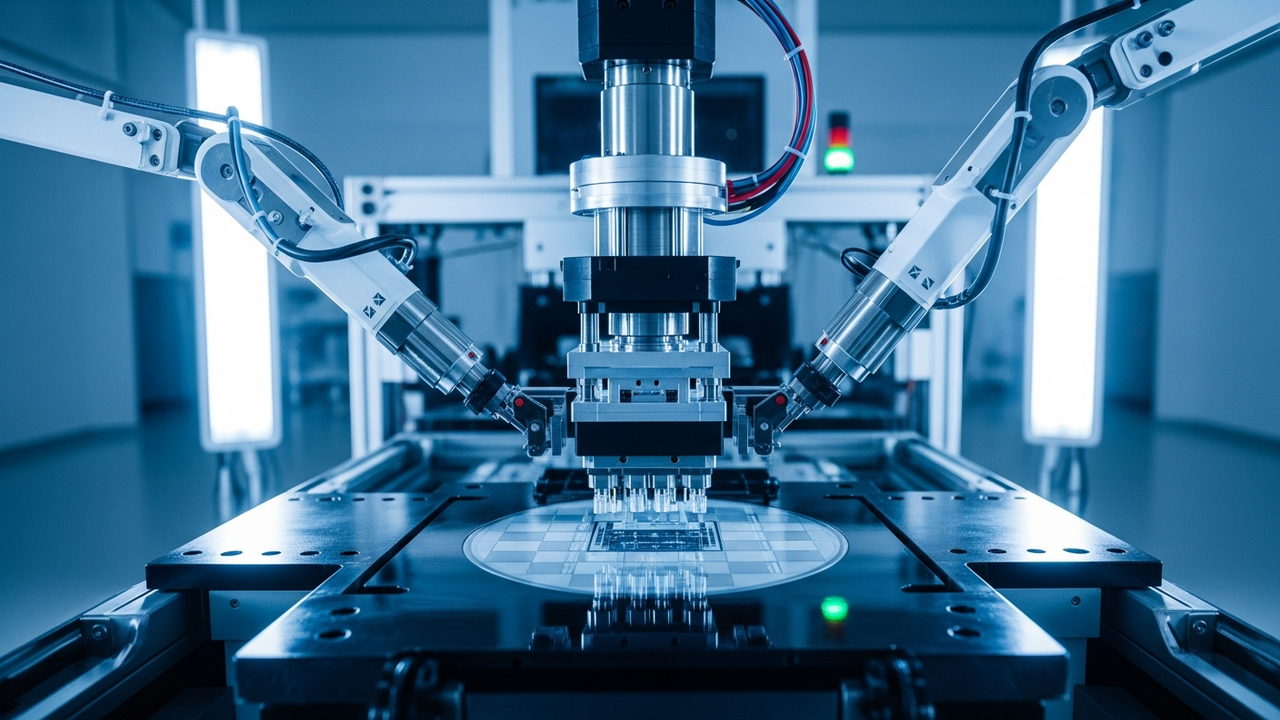
NIL operates by physically imprinting a nanoscale pattern from a master mold onto a resist layer, which is then cured using heat or UV light. Unlike optical lithography, NIL’s performance is not limited by light wavelength, allowing for significantly finer pattern resolution essential for sub-10 nm device fabrication. This physical transfer process offers inherent advantages in resolution and potentially lower operational expenses compared to increasingly complex and costly extreme ultraviolet (EUV) lithography systems. The technique is compatible with existing semiconductor fabrication processes, and hybrid systems combining NIL with traditional methods are being explored to optimize manufacturing workflows.
Background & Context
The semiconductor industry has relentlessly pursued Moore’s Law, doubling transistor density approximately every two years. However, conventional optical lithography is approaching its fundamental physical limits, and the escalating costs of advanced EUV systems pose significant economic challenges. NIL presents a compelling alternative, especially for applications like memory chips, where cost-effectiveness and high resolution are paramount. Companies such as Canon and Morphotonics are actively developing and commercializing NIL solutions, aiming to overcome the current scaling bottlenecks and drive innovation in advanced chip manufacturing.
Strategic Significance & Outlook
The widespread adoption of NIL could dramatically alter the economic landscape of semiconductor production, facilitating the development of more powerful and affordable chips. This would have profound implications for AI, IoT, and 5G technologies, which rely on ever-improving semiconductor performance. Further research and development are focused on overcoming challenges such as defect control, mold longevity, and ensuring pattern uniformity across large wafers. Successful integration of NIL could unlock new possibilities for miniaturization and functionality, securing its role as a cornerstone technology for the future of electronics.
Source: https://chipxpert.in/nanoimprint-lithography-for-future-chips/
Get our weekly technology intelligence — free
Receive an infographic that lets you judge at a glance whether each field’s analysis report is worth reading.
Subscribe Free — Weekly Tech Intelligence
By subscribing, you’ll receive Troy-Technical’s weekly technology intelligence newsletter.
- Your email and selected fields are used only to deliver the newsletter.
- We never share your information with third parties.
- You can unsubscribe anytime via the link in each email.
See our Privacy Policy for details.
Takes about a minute · Unsubscribe anytime




