Key Findings
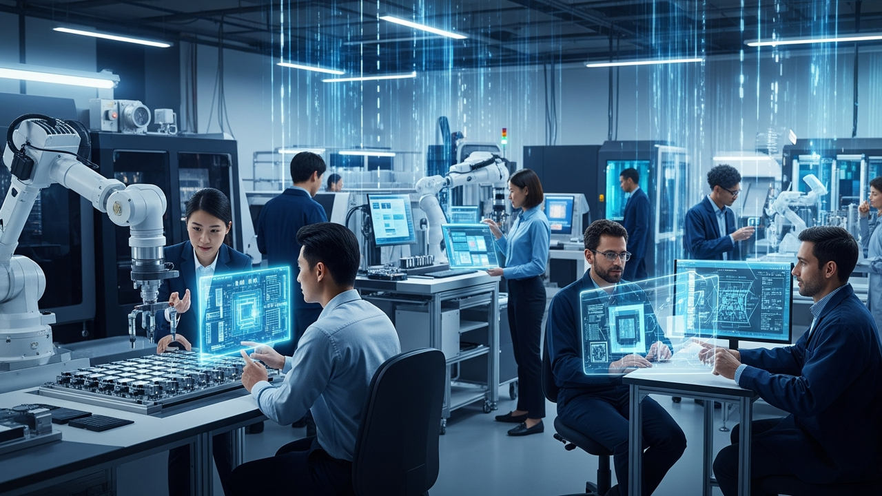
Henkel has unveiled the expansion and relocation of its Silicon Valley Application Center for Electronics to a larger site in Santa Clara, CA. This strategic move is intended to strengthen customer collaboration and significantly accelerate the development of new products. The expanded facility will prioritize research and development in key material technologies—such as underfills, structural adhesives, encapsulants, and thermal control solutions—which are indispensable for the advancement of artificial intelligence (AI) and high-performance computing (HPC).
Technical Details
The new Silicon Valley Application Center is equipped with state-of-the-art testing and analytical instruments, enabling the provision of advanced material solutions to address the complex challenges faced by electronics manufacturers. Specifically, efforts will focus on optimizing thermal management for high-performance processors and memory, improving underfill materials for stress relief in high-density packaging, and developing encapsulants for device protection in harsh environments. Research into structural adhesives, which facilitate dissimilar material bonding and lightweighting, will also be enhanced. These materials are crucial for ensuring the high reliability and long-term stability required by AI applications. The expanded center offers an environment where customers can closely collaborate with Henkel’s experts throughout the entire development cycle, from material selection to application testing and process optimization.
Background & Context
The rapid evolution of AI and HPC has dramatically increased the integration density and heat generation in electronic components, creating new challenges in the realm of materials science. Data centers, autonomous vehicles, next-generation mobile devices, and consumer electronics like XR/VR headsets all demand more high-performance and reliable adhesive, encapsulation, and thermal management materials. Silicon Valley stands as the global epicenter for these technological innovations, and Henkel’s strengthened presence in this region is a strategic move to respond quickly to market needs and secure a competitive advantage.
Strategic Significance & Outlook
Henkel’s expansion of its Silicon Valley Application Center represents a significant investment aimed at further solidifying its leadership in the electronic materials sector. This initiative is closely aligned with the growth of the AI and HPC markets, driving material innovations that will define the performance and reliability of next-generation electronic devices. New material solutions emerging from this center are expected to contribute to the realization of smaller, more powerful devices, enhance energy efficiency, and create more immersive XR/VR experiences. For investors and technologists, this serves as a clear indicator of Henkel’s sustained growth and innovation capabilities within the advanced electronic materials market.
Get our weekly technology intelligence — free
Receive an infographic that lets you judge at a glance whether each field’s analysis report is worth reading.
Subscribe Free — Weekly Tech Intelligence
By subscribing, you’ll receive Troy-Technical’s weekly technology intelligence newsletter.
- Your email and selected fields are used only to deliver the newsletter.
- We never share your information with third parties.
- You can unsubscribe anytime via the link in each email.
See our Privacy Policy for details.
Takes about a minute · Unsubscribe anytime




