Key Findings
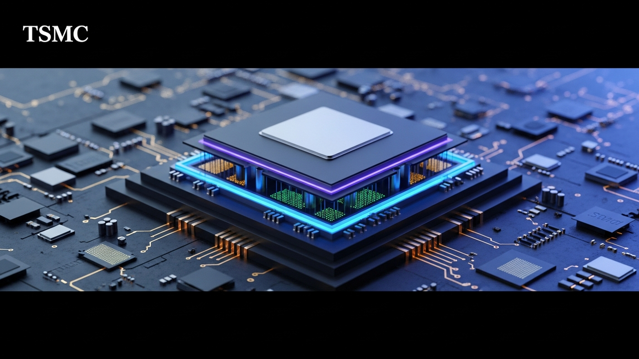
TSMC is reportedly collaborating with Kinsus to develop a new AI chip packaging technology similar to Intel’s Embedded Multi-die Interconnect Bridge (EMIB). This strategic move addresses the pressing issue of limited CoWoS (Chip-on-Wafer-on-Substrate) capacity, which is crucial for packaging high-end AI processors for key clients such as Nvidia and AMD.
Technical and Clinical Details
Traditional CoWoS technology, while highly effective for integrating multiple dies, relies on a full silicon interposer, which contributes to higher manufacturing costs, yield challenges, and capacity constraints. The EMIB-like approach bypasses the need for a full interposer by embedding smaller silicon bridges directly into the package substrate. This method allows for high-density interconnections between chips while offering several advantages: reduced manufacturing costs due to simplified processes, improved yields, and enhanced scalability for larger multi-die AI packages. The ability to efficiently integrate more chiplets is expected to significantly boost the performance and integration density of future AI accelerators, making them more powerful and cost-effective.
Background and Industry Context
The explosive growth of artificial intelligence has led to an unprecedented demand for high-performance AI chips. Nvidia’s GPUs and AMD’s AI accelerators, in particular, have become indispensable components in data centers and cloud AI services. However, the advanced packaging required for these chips, especially CoWoS, has faced significant production capacity limitations. This supply bottleneck has emerged as a critical constraint slowing the overall deployment of AI infrastructure. Consequently, leading foundries like TSMC have been under pressure to innovate and develop alternative packaging solutions to meet the burgeoning market demand.
Strategic Significance and Outlook
The joint development of this new packaging technology by TSMC and Kinsus is paramount for alleviating AI chip manufacturing bottlenecks and accelerating the mass production of next-generation AI hardware. A successful implementation of EMIB-like technology would lead to the availability of more powerful and cost-efficient AI processors, further driving the adoption and evolution of AI across industries. This development stands to benefit not only AI chip design companies such as Nvidia and AMD but also data center operators and AI application developers who rely on advanced hardware. The industry will be closely watching the maturation of this technology and the establishment of its mass production capabilities, as it could reshape the competitive landscape of AI hardware manufacturing.
Source: https://www.techinasia.com/news/tsmc-explores-new-ai-chip-packaging-with-kinsus
Get our weekly technology intelligence — free
Receive an infographic that lets you judge at a glance whether each field’s analysis report is worth reading.
Subscribe Free — Weekly Tech Intelligence
By subscribing, you’ll receive Troy-Technical’s weekly technology intelligence newsletter.
- Your email and selected fields are used only to deliver the newsletter.
- We never share your information with third parties.
- You can unsubscribe anytime via the link in each email.
See our Privacy Policy for details.
Takes about a minute · Unsubscribe anytime