Background
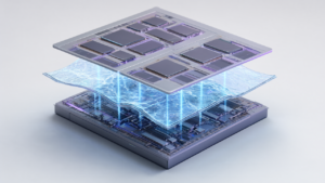
The exponential growth of artificial intelligence has created unprecedented demand in the semiconductor industry. AI accelerators, in particular, require more cores, High-Bandwidth Memory (HBM) stacks, and larger package sizes, pushing existing packaging technologies to their limits. CoWoS (Chip-on-Wafer-on-Substrate), while a de facto standard for advanced packaging, faces limitations in terms of production efficiency and cost for very large dies due to its wafer-based nature. Against this backdrop, Panel-Level Packaging (PLP) is gaining traction as a next-generation solution for integrating large accelerators with chiplet architectures and HBM stacks.
Key Findings
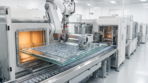
TSMC has initiated a pilot line for its innovative CoPoS (Chip-on-Panel-on-Substrate) advanced packaging technology at VisEra’s Longtan plant in Taiwan. This strategic move directly addresses the critical CoWoS production capacity bottlenecks currently impacting AI chip availability. The new CoPoS platform, leveraging 310x310mm rectangular glass panels, is slated for mass production between late 2028 and 2029.
Current CoWoS technology is fundamentally limited by the 12-inch wafer form factor, which restricts overall output and wafer-level packaging equipment capacity—a significant bottleneck for burgeoning AI chip demand. TSMC’s CoWoS capacity is reportedly fully booked through 2027 by major customers like Nvidia, AMD, and Google, underscoring the urgent need for alternative high-volume solutions.
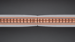
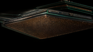
CoPoS transcends these 12-inch wafer limitations by employing Panel-Level Packaging (PLP), which offers significantly higher output per unit area. It capitalizes on existing display panel production lines, enabling rapid capacity expansion. Technically, CoPoS utilizes glass substrates, Physical Vapor Deposition (PVD), and high-precision panel-level lithography to achieve micron-level circuit accuracy. Its warpage-controlled, low-stress plastic packaging further facilitates the efficient tiling of large dies and high-density integration, crucial for demanding High-Performance Computing (HPC), 5G/6G, and AI applications. This approach becomes particularly advantageous for chip packaging areas exceeding 3.3 times the mask size, providing a pathway to overcome performance and cost bottlenecks.
TSMC’s CoPoS strategy aims to more efficiently tile larger AI dies, directly challenging competing technologies like Intel’s Embedded Multi-die Interconnect Bridge (EMIB). The introduction of CoPoS is expected to significantly change the AI chip manufacturing ecosystem by alleviating CoWoS supply constraints and potentially increasing AI chip availability in the market. The broader industry trend, evidenced by Intel’s collaboration with China’s Lens Technology on glass substrate-based advanced packaging (targeting 2H 2027 mass production), suggests that PLP with glass substrates is becoming a major competitive battleground. This technology is positioned to set new industry benchmarks for performance, cost, and production efficiency in the AI era, intensifying market competition. Furthermore, Taiwan’s supply chain, including companies like Innolux, AUO, and TPK-KY, is actively developing Fan-Out Panel-Level Packaging (FOPLP) using square glass substrates and Through-Glass Via (TGV) technology, signaling readiness for widespread CoPoS adoption.
Source: https://eu.36kr.com/en/p/3916013244558981
Get our weekly technology intelligence — free
Receive an infographic that lets you judge at a glance whether each field’s analysis report is worth reading.
Subscribe Free — Weekly Tech Intelligence
By subscribing, you’ll receive Troy-Technical’s weekly technology intelligence newsletter.
- Your email and selected fields are used only to deliver the newsletter.
- We never share your information with third parties.
- You can unsubscribe anytime via the link in each email.
See our Privacy Policy for details.
Takes about a minute · Unsubscribe anytime