Key Findings
The Professional Development Courses (PDCs) at the IMAPS Device Packaging Conference 2026 provided an in-depth exploration of “Advanced Packaging for Chiplets and Heterogeneous Integration,” underscoring this as one of the industry’s most critical technological trends. The courses distinctly defined various IC integration approaches, from 2D to 3.5D, based on interconnect density and electrical performance, with a specific focus on advancements in chiplet communication and hybrid bonding.
Technical / Clinical Details
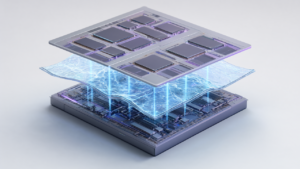
- Defining Chiplets and Heterogeneous Integration: The PDCs detailed various forms of IC integration, ranging from 2D packaging to 2.5D with high-density interposers, 3D involving direct die-to-wafer connections, and 3.5D combining build-up packages with bridge technologies. These were explained from the perspective of interconnect density and electrical performance, offering clear guidance for designers to select optimal integration approaches based on specific application requirements.
- Innovations in Chiplet Communication: Communication between chiplets is achieved through bridges, made of silicon or organic materials, embedded within build-up package substrates, or via fan-out epoxy molding compounds (EMCs) equipped with high-density Redistribution Layers (RDLs). These technologies enable high-speed and efficient data transfer between chiplets, thereby enhancing overall system performance.
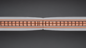
- Fundamentals and Applications of Hybrid Bonding: The basic principles of hybrid bonding were elaborated, explaining how this technology achieves ultra-fine pitch (sub-micron) die-to-wafer or die-to-die connections. Furthermore, concrete high-volume products leveraging this technology, such as smartphone processors and High Bandwidth Memory (HBM), were showcased, emphasizing its practical utility.
Background & Context
The demands of next-generation applications like AI, High-Performance Computing (HPC), and 5G/6G communications necessitate exponential increases in semiconductor chip complexity and performance. Traditional monolithic chip design faces limitations in manufacturing cost, yield, and design flexibility, leading chiplets and heterogeneous integration to emerge as primary industry solutions. These technologies enable performance improvements and cost optimization beyond Moore’s Law by manufacturing different functionalities as separate chiplets and then efficiently integrating them in the backend.
Strategic Significance & Outlook
The IMAPS Device Packaging Conference PDCs offered a valuable opportunity for researchers, engineers, and industry professionals to gain a deep understanding of the latest trends in chiplets and heterogeneous integration and to apply this knowledge to their product development. The proliferation of advanced connection technologies like hybrid bonding will further accelerate the evolution of high-density, high-performance applications, such as AI chips and HPC modules. Moving forward, these technologies are expected to become mainstream in semiconductor packaging, driving innovation across the entire electronics industry.
Source: https://imaps.org/page/DPC-26-PDCs
Get our weekly technology intelligence — free
Receive an infographic that lets you judge at a glance whether each field’s analysis report is worth reading.
Subscribe Free — Weekly Tech Intelligence
By subscribing, you’ll receive Troy-Technical’s weekly technology intelligence newsletter.
- Your email and selected fields are used only to deliver the newsletter.
- We never share your information with third parties.
- You can unsubscribe anytime via the link in each email.
See our Privacy Policy for details.
Takes about a minute · Unsubscribe anytime