Key Findings
The Professional Development Courses (PDCs) at the IMAPS (International Microelectronics Assembly and Packaging Society) Device Packaging Conference 2026 offered detailed insights into the forefront of current 3D IC and 2.5D IC packaging processes and technologies, as well as their future developmental trajectories. Particular attention was given to innovative techniques such as Fan-Out Panel Level Packaging (FOPLP), hybrid bonding, and copper pillar thermo-compression bonding. It was emphasized that these technologies are vigorously driving the demand for 3D IC and wafer-level packaging across diverse sectors, including mobile devices, high-performance data centers, automotive, and aerospace.
Technical / Clinical Details
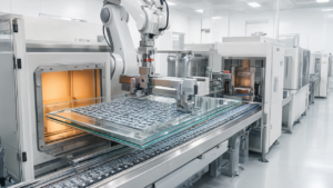
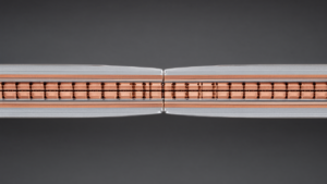
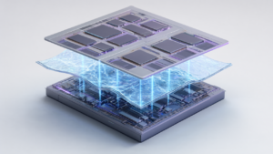
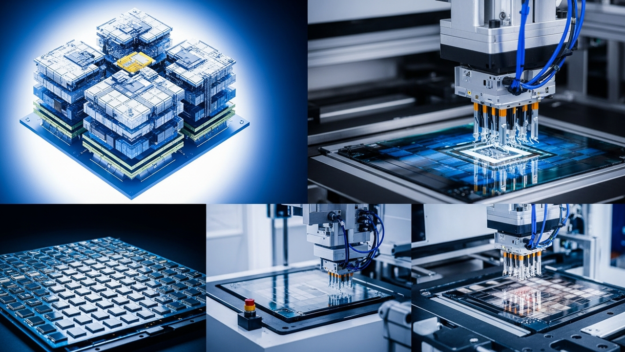
3D IC and 2.5D IC packaging achieve integration density and performance beyond the limits of traditional 2D packaging by integrating multiple semiconductor dies vertically or horizontally. FOPLP (Fan-Out Panel Level Packaging) is a technology that packages chips on larger square or rectangular panels rather than circular wafers, enabling improved material efficiency and reduced manufacturing costs. This approach provides high throughput and cost-effectiveness for large and complex packaging solutions required by HPC (High-Performance Computing) and AI accelerators. Hybrid bonding directly connects chiplets at sub-micron pitches via copper-to-copper bonds, dramatically increasing I/O density, maximizing data bandwidth, and improving power efficiency. This is crucial for integrating HBM (High Bandwidth Memory) with logic dies or for ultra-high-speed communication between chiplets. Copper pillar thermo-compression bonding connects chips via fine copper pillars, offering excellent electrical and thermal characteristics. These technologies provide high-density, high-performance, low-power, and reliable packaging solutions required by various applications, including server processors for data centers, AI chips for autonomous vehicles, SoCs (System-on-Chip) for next-generation mobile devices, and robust high-performance systems in the aerospace sector.
Background & Context
The semiconductor industry faces the challenge of slowing Moore’s Law, making it difficult to sustain performance improvements solely through transistor miniaturization. Consequently, packaging technology is being re-evaluated as a primary means to enhance system-level performance and functionality. Technological advancements in AI, 5G, IoT, and autonomous driving, in particular, are accelerating the development of chips that demand high integration, high performance, and low power consumption, thereby increasing the demand for advanced technologies like 3D/2.5D packaging, FOPLP, and hybrid bonding. Discussions at international forums like IMAPS indicate that these technologies are transitioning from research stages to practical implementation and are becoming established as industry standards.
Strategic Significance & Outlook
The advanced packaging technologies highlighted at IMAPS DPC 2026 are expected to continue shaping the major trends in the semiconductor industry for years to come. FOPLP will drive the market with its improved manufacturing cost efficiency and large-area capability, while hybrid bonding will lead with ultra-high-density interconnects. The widespread adoption of these technologies will enable further performance enhancements in mobile devices, increased processing power in data centers, strengthened real-time AI processing in autonomous vehicles, and the development of compact, high-reliability systems in the aerospace sector. As these technologies mature and gain broader adoption, a new wave of innovation in semiconductor chip design and manufacturing is anticipated. The industry must collaborate to maximize the opportunities presented by these technologies while overcoming remaining technical challenges (e.g., thermal management, yield, reliability).
Source: https://imaps.org/page/DPC-26-PDCs
Get our weekly technology intelligence — free
Receive an infographic that lets you judge at a glance whether each field’s analysis report is worth reading.
Subscribe Free — Weekly Tech Intelligence
By subscribing, you’ll receive Troy-Technical’s weekly technology intelligence newsletter.
- Your email and selected fields are used only to deliver the newsletter.
- We never share your information with third parties.
- You can unsubscribe anytime via the link in each email.
See our Privacy Policy for details.
Takes about a minute · Unsubscribe anytime