Key Findings
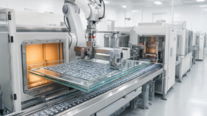
Samsung Electro-Mechanics has dramatically increased its average semiconductor package substrate utilization rate to 89% in the first half of this year, representing a substantial 19 percentage point jump year-over-year. This surge is primarily fueled by the exploding demand for AI data center infrastructure, with high-value Flip-Chip Ball Grid Array (FCBGA) substrates being a key driver for the company’s package solution division.
Technical Details
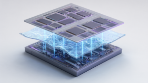
- A utilization rate of 89% indicates that Samsung Electro-Mechanics’ production lines are operating near full capacity, reflecting the tight supply conditions in the AI semiconductor market. FCBGA is a critical packaging technology used to connect high-performance logic chips like CPUs, GPUs, and AI accelerators with High Bandwidth Memory (HBM), growing in importance as AI workloads become more complex.
- This elevated operational efficiency underscores how investments in advanced packaging technology, crucial for maximizing AI semiconductor performance, are directly contributing to the company’s revenue and market share. The quality and stable supply of FCBGA are paramount for AI data centers that demand massive data processing and extremely high data transfer speeds.
Background & Context
The rapid advancement and adoption of AI technologies have dramatically amplified the demand for computing power in data centers worldwide. This has led to an explosive increase in AI semiconductor chip demand, with HBM and the advanced packaging substrates required for its implementation becoming significant bottlenecks in the supply chain. Samsung Electro-Mechanics’ soaring utilization rate is concrete evidence of the profound impact of this global AI boom across the entire semiconductor backend supply chain. As numerous global tech giants accelerate their AI strategies, a stable supply of high-performance package substrates is becoming a key competitive differentiator.
Strategic Significance & Outlook
Samsung Electro-Mechanics’ high utilization rate signals robust future growth in the AI semiconductor market and positions the company to capitalize on this expansion. However, sustained high utilization also strains the broader supply chain, carrying potential risks of shortages and price increases. The company is expected to continue expanding its production capacity for high-value products through ongoing capital investments and technological innovation to reinforce its leadership in the AI era.
Source: #
Get our weekly technology intelligence — free
Receive an infographic that lets you judge at a glance whether each field’s analysis report is worth reading.
Subscribe Free — Weekly Tech Intelligence
By subscribing, you’ll receive Troy-Technical’s weekly technology intelligence newsletter.
- Your email and selected fields are used only to deliver the newsletter.
- We never share your information with third parties.
- You can unsubscribe anytime via the link in each email.
See our Privacy Policy for details.
Takes about a minute · Unsubscribe anytime