Key Findings
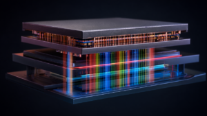
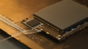
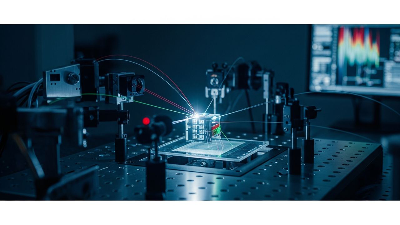
Researchers at Shanghai Jiao Tong University have developed an innovative reconfigurable germanium-silicon photodetector utilizing a low-loss integration strategy based on Fan-Out Wafer Level Packaging (FOWLP). This groundbreaking technology facilitates the seamless integration of electronic integrated circuits (ICs) and photonic ICs without the need for conventional wire bonding. This approach dramatically reduces parasitic losses and enhances signal integrity, marking a significant breakthrough in addressing the challenges of high-density interconnects and low insertion loss in optical communication systems, ultimately meeting the escalating demands of data centers.
Technical / Clinical Details
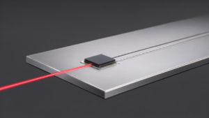
- **Reconfigurable Photodetector**: The developed germanium-silicon photodetector features “reconfigurability,” meaning its characteristics can be dynamically adjusted to meet diverse optical signal processing requirements. This enhances system design flexibility and efficiency. Germanium offers superior absorption efficiency over a broader wavelength range than silicon, particularly in the near-infrared spectrum, making it highly effective for the primary communication wavelengths used in data centers.
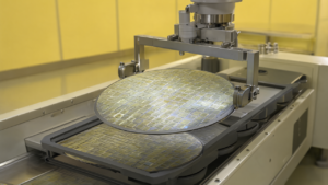
- **Fan-Out Wafer Level Packaging (FOWLP)**: FOWLP is an advanced semiconductor packaging technology where chips are embedded directly onto a wafer, encapsulated in resin, and then interconnected via redistribution layers. Adopting this technology provides several key benefits:
- **Elimination of Wire Bonding**: Compared to traditional wire bonding, FOWLP significantly shortens electrical paths, reducing parasitic capacitance and inductance. This minimizes signal degradation in high-speed data transmission.
- **High-Density Integration**: FOWLP enables the high-density integration of multiple chips (both electronic and photonic ICs) to realize system miniaturization and increased interconnect density.
- **Low Insertion Loss**: Signal losses at the electronic-optical interface are minimized, improving the overall efficiency of the optical communication system.
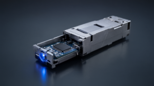
- **Data Center Application**: Data centers increasingly require faster and more power-efficient interconnects for data transmission within and between server racks. This technology serves as a foundational element for realizing terabit-class optical transceivers and Co-Packaged Optics (CPO), expected to meet the vast data bandwidth and low power consumption demands of AI/ML workloads.
Background & Context
With the advent of AI and High-Performance Computing (HPC), data traffic within data centers has surged exponentially. Traditional electrical interconnects based on copper wires are now facing limitations in terms of power consumption, latency, and bandwidth. Consequently, the transition to optical interconnects is inevitable, and there is an urgent need for photonic-electronic integration technologies that more closely combine electronic and optical circuits. Efficient packaging techniques are pivotal for achieving this integration.
Strategic Significance & Outlook
The research achievement from Shanghai Jiao Tong University marks a critical step forward in photonic-electronic integration. The reconfigurable germanium-silicon photodetector, enhanced by FOWLP, holds the potential to dramatically improve the performance and efficiency of next-generation optical interconnects in data centers. Further development and mass production of this technology could contribute to cost reduction and miniaturization of optical transceivers, thereby accelerating the widespread deployment of AI infrastructure. In the future, this technology is also anticipated to find applications in more complex optical signal processing and advanced fields like quantum photonics.
Source: https://www.photonics.com/Articles/Advanced-Packaging-Simplifies-Complex/a72271
Get our weekly technology intelligence — free
Receive an infographic that lets you judge at a glance whether each field’s analysis report is worth reading.
Subscribe Free — Weekly Tech Intelligence
By subscribing, you’ll receive Troy-Technical’s weekly technology intelligence newsletter.
- Your email and selected fields are used only to deliver the newsletter.
- We never share your information with third parties.
- You can unsubscribe anytime via the link in each email.
See our Privacy Policy for details.
Takes about a minute · Unsubscribe anytime