Key Findings
TSMC Vice President Ho Chun publicly announced that multiple AI-related products, assembled using the company’s CoWoS (Chip-on-Wafer-on-Substrate) 5.5x reticle size process, are achieving an impressive yield rate of 98% to 99%. This figure unequivocally demonstrates TSMC’s superior manufacturing efficiency and quality in the highly intricate field of heterogeneous integration packaging for AI chips. Furthermore, Vice President Ho unveiled an ambitious roadmap to significantly expand CoWoS technology from its current 5.5x to a 14x reticle size by 2029.
Technical / Clinical Details
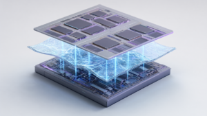
CoWoS is a critical 2.5D packaging technology essential for maximizing the performance of AI accelerators by integrating high-performance logic dies with HBM (High Bandwidth Memory) on a silicon interposer. Achieving 98-99% yield in this technology signifies TSMC’s mature process control capabilities and advanced automation in micro-bump flip-chip bonding, silicon interposer fabrication, and subsequent packaging stages. Challenges associated with scaling packaging capabilities to over three times the photomask size include managing warpage in large interposers, ensuring the integrity of multi-layer structures, and addressing the complexities of thermal management. TSMC’s planned expansion to a 14x reticle size is crucial for integrating even more AI chiplets and HBM stacks within a single package, thereby meeting the massive computational power and memory bandwidth demands of next-generation AI models. This scale-up necessitates further innovations in manufacturing equipment, materials, and process technology.
Background & Context
The rapid evolution of AI, particularly generative AI, has fueled an explosive demand for high-performance AI semiconductors. For these AI chips, not only computational power but also memory bandwidth and efficiency are paramount, making advanced packaging technologies like CoWoS a critical bottleneck. TSMC’s achievement of high yields demonstrates its capacity to meet these challenging market requirements and contributes to stabilizing the supply of AI chips. While competitors are also accelerating investments in advanced packaging, TSMC’s CoWoS technology maintains its position as an industry benchmark. This announcement reassures investors and customers of TSMC’s long-term strategy to address future AI demand, bringing stability to the entire semiconductor supply chain.
Strategic Significance & Outlook
The continuous evolution of TSMC’s CoWoS technology, especially its expansion to a 14x reticle size by 2029, will elevate AI chip performance and integration density to new levels. This will enable the training and inference of larger and more complex AI models, further broadening the application scope of AI. However, the advancement of such large-scale packaging technologies simultaneously requires innovations in substrate materials, cooling solutions, and testing methodologies. TSMC’s CoWoS strategy will not only solidify its leadership in the AI era but also profoundly influence the overall technology roadmap and competitive landscape of the semiconductor industry.
Source: https://wccftech.com/tsmc-exec-makes-big-announcement-confirms-98-yield-for-cowos-packaged-ai-chips/
Get our weekly technology intelligence — free
Receive an infographic that lets you judge at a glance whether each field’s analysis report is worth reading.
Subscribe Free — Weekly Tech Intelligence
By subscribing, you’ll receive Troy-Technical’s weekly technology intelligence newsletter.
- Your email and selected fields are used only to deliver the newsletter.
- We never share your information with third parties.
- You can unsubscribe anytime via the link in each email.
See our Privacy Policy for details.
Takes about a minute · Unsubscribe anytime