Key Findings
The University of California, Berkeley, has announced its participation in Applied Materials’ EPIC (Electronics Process Innovation & Collaboration) Center. This strategic partnership is set to significantly accelerate chip innovation by fostering advanced research and development collaboration and cultivating next-generation talent, particularly in the critical areas of advanced packaging and materials science for semiconductors.
Technical / Clinical Details
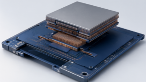
UC Berkeley’s involvement in the EPIC Center will amplify research efforts focused on developing novel materials, process technologies, and advanced packaging solutions essential for achieving higher performance and energy efficiency in future semiconductor devices. Key areas of focus include heterogeneous integration, 3D stacking techniques, and innovative bonding methods, which are vital for overcoming the physical limitations of traditional chip scaling. By synergizing academic insights with Applied Materials’ industrial expertise and shared laboratory resources, the collaboration aims to drive breakthrough innovations. Furthermore, a crucial aspect of this partnership is the acceleration of engineering talent development, addressing the critical need for skilled professionals in the rapidly evolving semiconductor industry.
Background & Context
The relentless demand from AI, machine learning, and high-performance computing applications is pushing the boundaries of semiconductor chip performance. As traditional silicon scaling faces increasing challenges, advanced packaging solutions and novel materials have emerged as pivotal frontiers for enhancing chip performance, power efficiency, and cost-effectiveness. Applied Materials, a leader in materials engineering and process solutions, is proactively engaging with top-tier research institutions like UC Berkeley to address these complex challenges and strengthen the innovation ecosystem. Such collaborations are vital for bridging the gap between fundamental research and practical application, accelerating the commercialization of cutting-edge technologies.
Strategic Significance & Outlook
This collaboration between UC Berkeley and Applied Materials is expected to have a profound impact on accelerating the semiconductor technology roadmap, ensuring that future computing needs for the AI era are met. Advances in advanced packaging and materials research will enable the development of smaller, more powerful, and energy-efficient chips, driving innovation across a broad spectrum of applications including data centers, mobile devices, and autonomous vehicles. Moreover, the focus on nurturing exceptional talent will yield long-term benefits for the sustainable growth and competitiveness of the entire semiconductor industry, positioning both organizations at the forefront of technological progress.
Get our weekly technology intelligence — free
Receive an infographic that lets you judge at a glance whether each field’s analysis report is worth reading.
Subscribe Free — Weekly Tech Intelligence
By subscribing, you’ll receive Troy-Technical’s weekly technology intelligence newsletter.
- Your email and selected fields are used only to deliver the newsletter.
- We never share your information with third parties.
- You can unsubscribe anytime via the link in each email.
See our Privacy Policy for details.
Takes about a minute · Unsubscribe anytime