Background: The Cutting-Edge Race in Semiconductor Lithography
The evolution of semiconductor manufacturing technology forms the bedrock of modern digital society. Lithography, in particular, is the most critical process for miniaturizing circuit lines on chips, directly determining semiconductor performance and cost. Currently, extreme ultraviolet (EUV) lithography dominates leading-edge chip manufacturing, but EUV entails exceptionally high upfront costs and requires complex equipment and infrastructure. Consequently, Nanoimprint Lithography (NIL) has garnered attention as a potentially lower-cost and more efficient alternative.
Key Findings / Results: Challenges of Nanoimprint Lithography Compared to EUV
The Bits&Chips article suggests that despite its numerous advantages, Nanoimprint Lithography (NIL) is unlikely to directly replace EUV lithography in leading-edge chip manufacturing in the near future. NIL forms circuits by directly pressing a master mold onto a pattern layer. Unlike optical EUV, NIL is not limited by wavelength resolution, and can, in principle, create extremely fine patterns. Furthermore, NIL boasts significantly lower equipment costs and lower power consumption compared to EUV.
However, NIL faces several key technical challenges:
- Mask (Mold) Durability: Since NIL involves direct contact between the master mold and the substrate, wear and damage to the mold are unavoidable. Long-term stability, especially in high-volume manufacturing environments, remains a significant challenge. Balancing mold lifespan with manufacturing costs is crucial. For instance, mold defects can rapidly propagate across thousands of imprinted wafers.
- Defect Management and Yield: Nanoscale defects (e.g., microscopic particle adhesion, incomplete imprints) directly impact chip yield. Achieving defect management levels comparable to EUV, and ensuring high-yield mass production, requires advanced technical solutions. Current defect rates for NIL are still higher than those acceptable for advanced logic.
- Scalability: Leading-edge chip manufacturing demands extremely uniform imprinting across the entire wafer. Achieving uniform pressure and material filling across large wafer sizes (e.g., 300 mm) is technically challenging, and establishing robust process scalability is a significant hurdle. Maintaining overlay accuracy within sub-nanometer tolerances over large areas is particularly difficult.
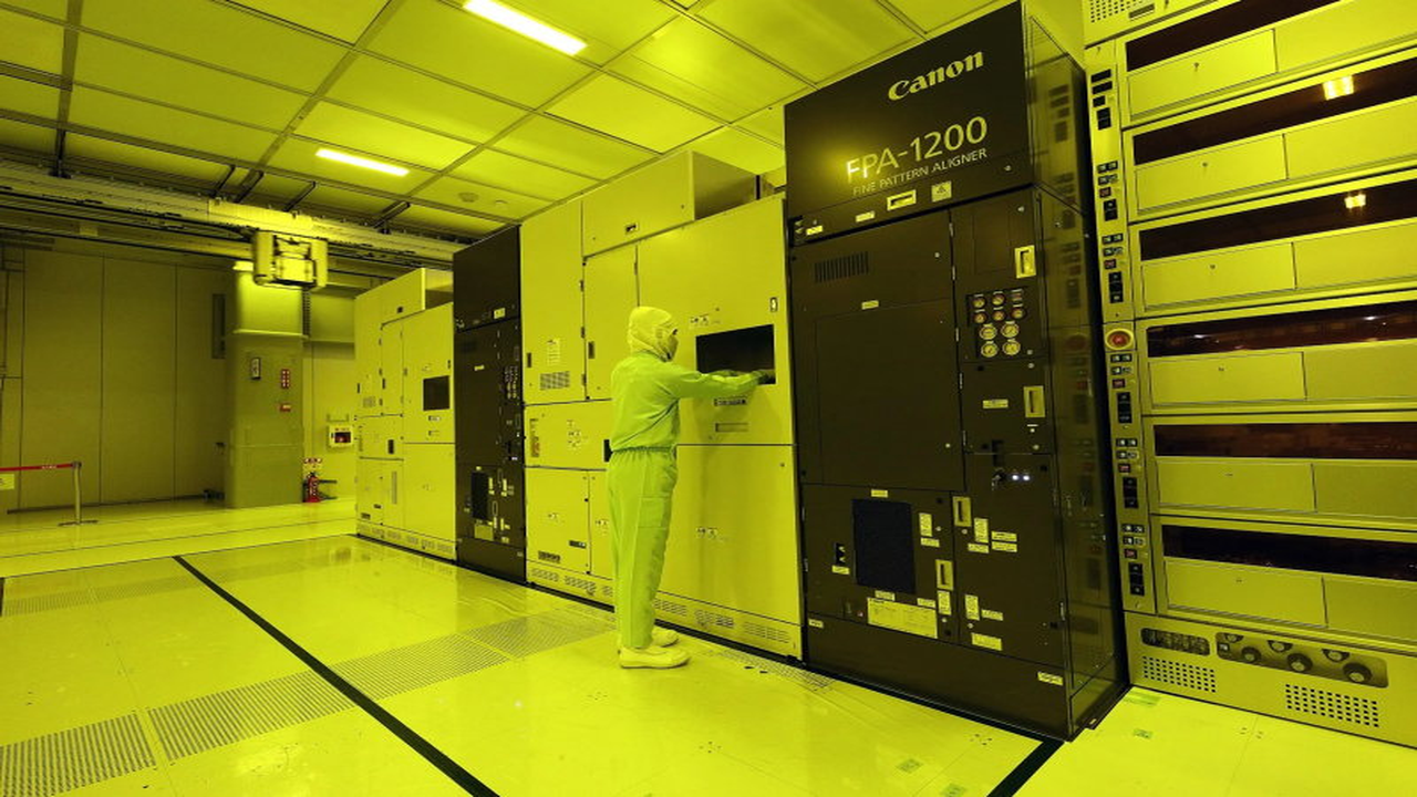
Japan’s Canon has been developing NIL technology for over two decades, claiming its capabilities extend to 5nm nodes and even more advanced chips. Canon’s “J-FIL (Jet and Flash Imprint Lithography)” technology attempts to overcome these challenges by combining drop-on-demand resist dispense with UV curing.
Technical Significance & Outlook: Niche Markets and Future Potential
This article suggests that NIL will likely not directly compete with EUV but will instead leverage its strengths in specific niche markets and applications where EUV is technically or economically prohibitive. For example, NIL could be advantageous in manufacturing NAND flash memory, which requires high-density patterns but less complex multi-layer interconnects than logic chips. Other potential areas include micro-LEDs, advanced optical devices, and MEMS sensors, where NIL’s cost-effectiveness and resolution are highly beneficial.
In the long term, with continued improvements in mask durability, defect reduction technologies, and optimized production throughput, NIL could become applicable to a broader range of semiconductor manufacturing. It may establish itself as a complementary technology to EUV, or even a substitute in specific domains, particularly for back-end-of-line (BEOL) processes or non-critical layers. Ongoing R&D investments by companies like Canon will be key to unlocking NIL’s full potential and reshaping the semiconductor manufacturing landscape.
Source: https://bits-chips.com/article/nanoimprint-lithography-wont-compete-with-euv-anytime-soon/









Comments