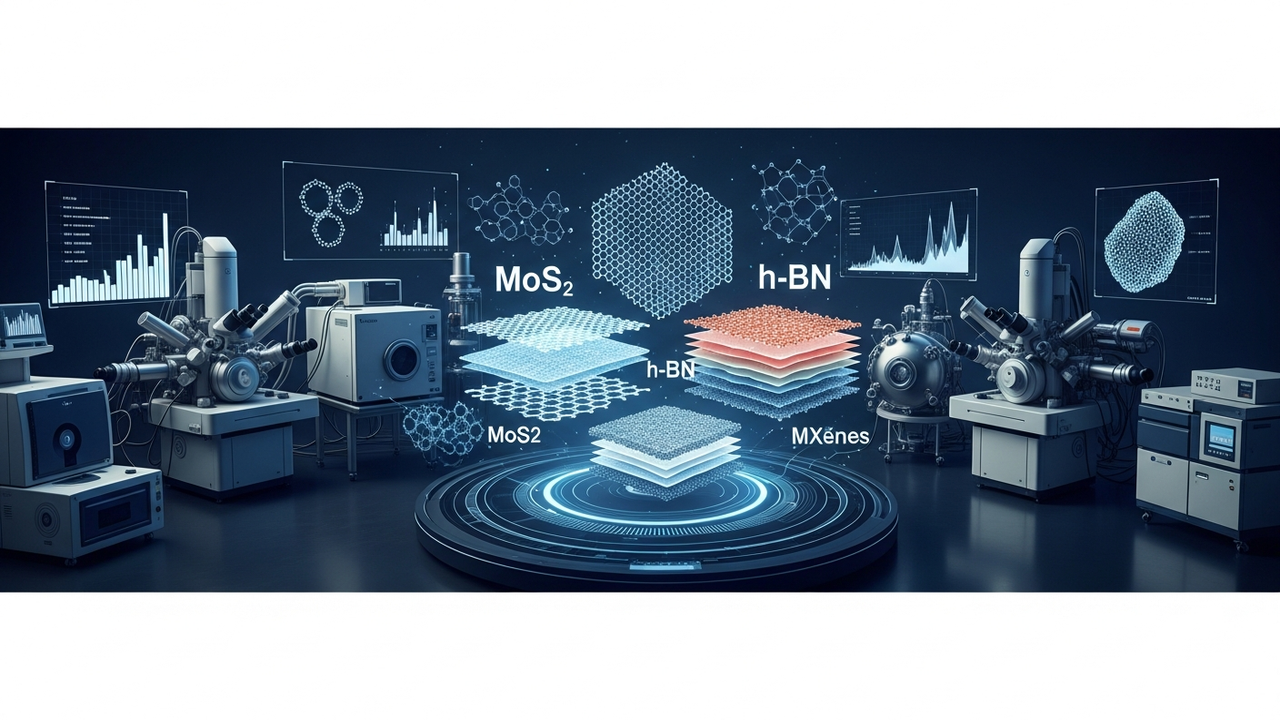
Background: 2D Materials Paving the Way for Next-Generation Technologies
Two-dimensional (2D) materials, exemplified by graphene, are poised to enable transformative applications across electronics, energy, healthcare, and composite materials due to their unique physical and chemical properties. Being atomically thin yet possessing exceptional electrical conductivity, mechanical strength, and optical transparency, these materials hold the potential to dramatically enhance the performance of next-generation devices. However, the transition from laboratory discovery to widespread industrial application requires establishing scalable manufacturing techniques and fostering innovations that maximize each material’s inherent characteristics.
Key Findings / Results: The 2026 Outlook and Key Trends in 2D Materials
The “2D Materials Landscape 2026” report published by PatSnap Eureka provides a detailed analysis of technological innovations and market trends focusing on four key 2D materials: graphene, molybdenum disulfide (MoS2), hexagonal boron nitride (h-BN), and MXenes. The primary findings from the report are as follows:
- Key Innovation Vectors: R&D efforts in 2D materials are predominantly directed towards:
- Device Performance Optimization: Enhancing the performance of 2D materials in various electronic and optoelectronic devices, including transistors, sensors, and LEDs.
- Multifunctionality: Creating hybrid materials with novel functions and properties by stacking or combining multiple 2D materials (heterostructures).
- Cost Reduction and Quality Improvement: Advancing synthesis techniques to produce high-quality 2D materials at scale and lower cost, crucial for industrial adoption.
- Frontiers of Synthesis Technology: 2D material manufacturing technologies are evolving from lab-scale manual exfoliation methods to wafer-scale chemical vapor deposition (CVD), with a strong focus on industrial applications. Research is particularly active in techniques for forming large-area, uniform, high-quality films. For example, wafer-scale graphene growth on 300mm substrates is becoming a reality, enabling integration into semiconductor processing.
- Patent Activity: The 2D materials sector exhibits robust patenting activity, with graphene leading in terms of patent family count. This indicates strong recognition of graphene’s broad application potential and commercial value, reflecting intense R&D and intellectual property protection efforts globally.
- Characteristics and Applications of Each Material Family:
- Graphene: Widely applied in electronics, energy storage, and composites due to its outstanding electrical (up to 200,000 cm²/Vs mobility) and thermal conductivity, and mechanical strength (tensile strength ~130 GPa).
- MoS2: Possessing semiconducting properties, MoS2 is promising for transistors, photodetectors, and catalysts, offering tunable bandgaps (1.2-1.8 eV).
- h-BN (White Graphene): Critical for graphene devices as a dielectric layer and for thermal management due to its excellent insulating properties and high thermal conductivity.
- MXenes: An emerging class of 2D transition metal carbides/nitrides, known for high electrical conductivity, hydrophilicity, and diverse chemical compositions, promising for energy storage (supercapacitors, batteries), electromagnetic shielding, and sensors. Their unique surface terminations (e.g., -OH, -O, -F) allow for highly tunable properties.
Technical Significance & Outlook: 2D Materials Driving Innovation and Industrial Future
The PatSnap Eureka report suggests that 2D materials will continue to exert a significant impact across diverse industrial sectors in the coming years. The technical maturation and establishment of scalable manufacturing methods for key materials like graphene, MoS2, h-BN, and MXenes will accelerate the development of next-generation semiconductors, high-performance batteries, flexible electronics, and highly sensitive sensors.
The vibrant patent activity reflects the pace of commercial competition and innovation in this field. Future keys to widespread industrial application will include improvements in defect control, uniformity, and yield for material production. Furthermore, standardization efforts for integrating 2D materials into existing technologies will gain increasing importance. 2D materials are not just novel substances but foundational technologies that will underpin new digital infrastructure, making their continued evolution a critical area of global technological focus.
Source: https://www.patsnap.com/resources/blog/mse-blog/2d-materials-landscape-2026-patsnap-eureka/







Comments