Background: Diversification of Semiconductor Manufacturing and Emerging Needs
The modern semiconductor industry is expanding beyond traditional microprocessor and memory chip manufacturing into diverse application areas such as augmented reality (AR), advanced 3D sensing, high-speed data communication, and biotechnology. These new fields demand specific material properties, three-dimensional structures, or ultra-fine patterns that are challenging to achieve with conventional silicon-based CMOS processes. In this context, Nanoimprint Lithography (NIL) is gaining attention as a cost-effective manufacturing technology adaptable to various materials.
Key Findings / Results: Diverse Applications of NIL in Semiconductor Devices
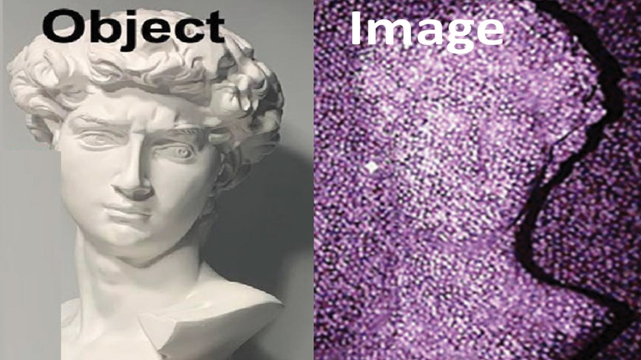
The Compound Semiconductor News article explores how Nanoimprint Lithography (NIL) can unleash its full potential across a wide range of semiconductor devices, extending beyond its traditional role in silicon MOSFET fabrication. NIL, leveraging a physical pattern transfer mechanism, is not constrained by optical diffraction limits and is capable of forming extremely fine nanostructures.
The key application areas and advantages of NIL highlighted in the article include:
- Augmented Reality (AR) Devices: NIL is well-suited for manufacturing lightweight and highly efficient diffractive optical elements (DOEs) and metasurfaces required for AR glasses and head-up displays. It can form the minute structures comprising these optical elements with high throughput and cost-efficiency, critical for mass production.
- Advanced 3D Sensing: For 3D sensing devices such as Time-of-Flight (ToF) sensors and structured light sensors found in smartphones and autonomous vehicles, NIL can be used for precise nanofabrication of optical components like VCSEL (Vertical-Cavity Surface-Emitting Laser) arrays and optical gratings. This enables more compact and higher-performance sensing modules.
- High-Bandwidth Datacom/Telecom: In the fabrication of silicon photonics and optoelectronic integrated circuits (PICs) using III-V compound semiconductors, NIL contributes to the high-precision formation of nanoscale waveguides, resonators, and couplers. This is indispensable for achieving high-speed and high-capacity data centers and 5G/6G communication networks.
- Biotechnology Devices: NIL is also applied in creating microstructures for biochips used in manipulating and detecting biomolecules, such as DNA sequencing chips, microfluidic devices, and cell culture scaffolds. NIL allows for direct patterning onto biocompatible materials, a significant advantage.
- Material Flexibility and Cost-Effectiveness: NIL offers flexibility in handling diverse materials, including silicon, compound semiconductors, polymers, and glass. Moreover, compared to EUV lithography, NIL boasts significantly lower equipment and operational costs, accelerating the practical implementation of new technologies.
- AI-Driven Design Methodologies: The article notes that AI-powered design automation tools are further accelerating the design and optimization of complex nanostructures for NIL, enhancing its manufacturing capabilities by reducing design cycle times and improving pattern fidelity.
Technical Significance & Outlook: NIL Opening Diverse High-Functionality Device Markets
The wide-ranging applicability of Nanoimprint Lithography will have a significant impact on the market for high-functionality devices. Especially in growing sectors like AR, 3D sensing, high-speed communication, and biotechnology, NIL provides high-precision and cost-effective manufacturing solutions that were difficult to achieve with conventional technologies. This will drive miniaturization, performance enhancement, and cost reduction of products in these fields, fostering market expansion.
NIL’s material versatility, scalability, and integration with AI will accelerate the cycle of technological innovation, enabling the creation of previously unimaginable new devices. This indicates that NIL will play a central role as the semiconductor industry moves into new frontiers of value creation. As international manufacturers focus on this technology, further evolution of NIL is expected to be key in shaping the future digital society, supporting a wide range of high-tech industries globally.
Source: https://compoundsemiconductor.net/article/122291/Unleashing_the_potential_of_nanoimprint_lithography







Comments